
Printed Circuit Boards (PCBs) and Printed Circuit Board Assemblies (PCBAs) are central components of the electronics manufacturing industry, directly impacting the performance and reliability of modern electronic products. According to a report by Fortune Business Insights, the global electronics manufacturing services market is projected to reach $797 billion by 2029, reflecting a remarkable 58% growth from 2022. This significant increase underscores the vital role of electronics manufacturing in the global economy.
To develop useful and appealing electronic products, optimizing the PCBA manufacturing process is crucial for every business. However, this task is not without challenges, as it involves multiple steps, from designing the circuit board layout to selecting the right components and final assembly. Each step demands a high level of precision and attention to detail. During the design phase, it is essential to consider both the circuit’s functionality and manufacturability, while component selection must balance performance and cost. The assembly process ensures that all parts are seamlessly connected.
Despite these challenges, by prioritizing efficient manufacturing processes, companies can expect to deliver high-quality PCBAs on time, gaining a competitive edge in the market. Achieving excellence in PCBA production not only enhances product quality but also allows businesses to shorten lead times and reduce production costs. By adopting advanced manufacturing technologies and continuously optimizing processes, companies can create more reliable and innovative electronic products that meet the ever-evolving demands of customers and market trends.
In this fast-paced industry, the continuous pursuit of excellence is key to achieving success. Investing in optimizing the PCBA manufacturing process means investing in the future, enabling businesses to remain competitive in a fiercely contested market.
A Deep Dive into the PCBA Manufacturing and Assembly Process
The manufacturing and assembly process of PCBA (Printed Circuit Board Assembly) is a critical component in ensuring the high quality and efficiency of electronic products. This process typically consists of several stages, each vital to the success of the final product.
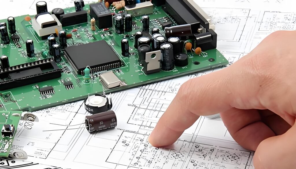
- Design Phase: In this stage, ideas are transformed into concrete blueprints through schematic diagrams and detailed design files. This not only includes the layout of the circuits but also the selection of appropriate components and materials. Effective design will directly impact the efficiency and quality of the subsequent production stages.
- Manufacturing Phase: Digital design files are then translated into physical blank PCBs. This step requires high precision to ensure that the circuit board accurately reflects the design intentions. Any minor errors during manufacturing can lead to significant issues later on, making accuracy crucial.
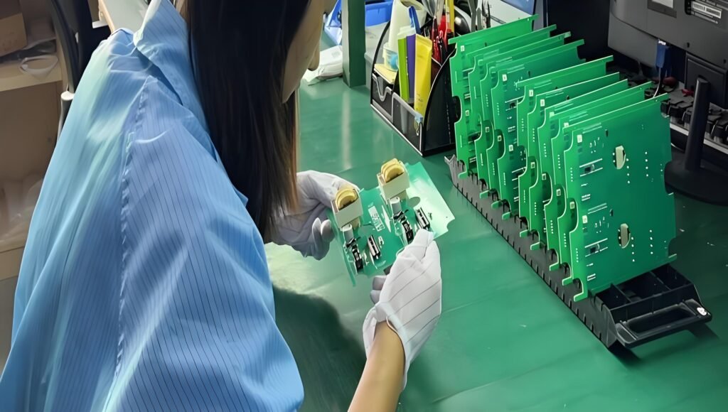
- Assembly Phase: During this stage, the PCB is populated with various components to achieve its intended functionality. This process includes soldering, placing, and securing components, ensuring that each element is firmly connected to the circuit board.
- Testing Phase: After assembly, all components must undergo rigorous testing to ensure they operate correctly. This includes functional tests, electrical tests, and performance evaluations to identify potential faults.
- Quality Control: Throughout the PCBA formation process, quality control ensures that products meet standards through assessments and inspections. Early defect detection at this stage can significantly reduce rework and repair costs.
While the process may appear straightforward, you may encounter unique challenges and requirements during actual operations. For example, the design phase may require frequent iterations to meet all technical specifications. The manufacturing and assembly stages will also need effective tools and technologies to ensure precision and efficiency at each step.
In this blog post, we will provide a detailed overview of each step and explain its significance in the broader PCB manufacturing and assembly process. Additionally, we will highlight relevant tools and technologies that can help you achieve the desired results. By understanding this information and leveraging the latest technologies, you can produce reliable and innovative electronic products that meet today’s market demands, thereby gaining a competitive edge.
Common Terminology: Definitions and Explanations
What is a PCB?
A Printed Circuit Board (PCB), also known as a Printed Wiring Board (PWB), is a fundamental component made from non-conductive materials, featuring conductive copper traces laid out on its surface. Its primary function is to connect various electronic components, such as resistors, capacitors, and integrated circuits, thereby forming a complete and functional electronic circuit. The design of a PCB not only facilitates circuit miniaturization but also enhances assembly efficiency, making it an indispensable part of nearly all electronic devices. From simple household appliances to complex computer systems, PCBs play a crucial role in modern electronic equipment.
What is PCBA?
PCBA, or Printed Circuit Board Assembly, refers to the result of soldering or assembling electronic components onto a PCB, forming a fully functional circuit component. This process typically involves connecting elements such as resistors, capacitors, and integrated circuits to the PCB using Surface Mount Technology (SMT) or Through-Hole Technology (PTH). PCBA is a critical step that ensures all components are interconnected and the circuit operates as intended. Whether in small consumer electronics or complex industrial machinery, PCBA is at the core of functionality.
What is the Difference Between PCB and PCBA?
While PCBs and PCBAs may appear similar, they are in fact at different stages of production. A PCB refers to the circuit board itself, focusing on the conductive traces and circuit design, while PCBA refers to all electronic components that have been fully assembled and soldered onto the PCB. In simple terms, a PCB is an unassembled circuit board, while a PCBA is a completed electronic component ready for use. Understanding the distinction between these two is vital in the electronic manufacturing and assembly process, as their functions and applications differ significantly. The PCB serves as the foundation, whereas the PCBA represents the realization of functionality.
Key Steps in the PCBA Design Process
The PCBA (Printed Circuit Board Assembly) design process is crucial for transforming abstract concepts into tangible, manufacturable products. This stage sets the foundation for all subsequent manufacturing steps and significantly impacts the final production results. Below are the key steps in the PCBA design process, each containing rich details and technical requirements.
1. Schematic Development
In this phase, engineers create a detailed blueprint that describes the relationships and functionalities of various electrical components on the circuit board. Although it may seem feasible to skip this step for simple products, the accuracy and completeness of the schematic are critical for complex devices. The schematic serves as the core of the entire design, dictating the circuit’s logic and operation.
2. Schematic Capture and Synchronization
Next, designers need to “capture” the created schematic into the PCBA layout. This step involves arranging and connecting components in a digital representation of the circuit board. Utilizing schematic capture tools can significantly expedite this process, ensuring seamless synchronization between the schematic and layout files, thereby reducing errors and enhancing design efficiency.
3. PCB Layer Stack Design
The PCB layer stack design involves the configuration of copper traces and insulating layers. This is vital for minimizing impedance issues, which can adversely affect device performance. Engineers must consider the distribution of power and signal layers to meet specific electromagnetic compatibility (EMC) requirements, thus optimizing signal integrity.
4. Design Rule Definition
Once the layer stack is established, it is essential to define the design rules for the PCBA. These rules encompass spacing between components, trace width, manufacturing limitations, and safety distances from the edges of the circuit board. Defining design rules helps ensure consistency and accuracy during the manufacturing process, thereby reducing the risk of rework.
5. Component Placement
Component placement is a critical step in the design process. Designers can utilize exploratory data analysis (EDA) tools for automated placement or manually arrange components in design software. The correct placement of components directly impacts the circuit’s performance and reliability, making it vital for maximizing signal transmission efficiency.
6. Hole Insertion
Following component placement, the next step is to insert holes for component mounting and vias. As the design evolves, the positions of these holes may need adjustment to ensure optimal electrical connections and mechanical stability. This step is crucial for guaranteeing accurate installation of components.
7. Routing
Routing in PCBA refers to the copper traces that transmit signals or power to various components. Accurate and precise routing is essential for the overall functionality of the device, and designers must carefully consider the layout of each trace to avoid signal interference and delays.
8. Labeling and Identification
Once routing is completed, labels and identifiers should be added to the circuit board to facilitate troubleshooting and design modifications in the future. This step enhances maintenance efficiency and reduces the likelihood of errors occurring.
9. Design File Generation
The final step involves generating the design files that form the basis for manufacturing and assembly. These files typically include Gerber/ODB++ files, a Bill of Materials (BOM), and centroid (X, Y position) files. These documents are essential for ensuring the accurate production of PCB components, as even minor errors can lead to production delays or increased costs.
By following these key steps and leveraging the latest technologies and design tools, you can efficiently produce high-quality, reliable PCBA that meets specific requirements. This process not only emphasizes the importance of accuracy and attention to detail in design but also highlights the complexity and challenges of electronic manufacturing. By continually optimizing the design process, you can maintain a competitive edge and meet the growing demands for electronic products in the market.
Key Considerations in PCBA Design
When developing complex electronic products that incorporate PCBA (Printed Circuit Board Assembly), it is crucial to maintain a focus on the manufacturing and assembly processes. Here are some important factors that can help streamline your workflow and enhance overall project efficiency:
1. Component Availability and Pricing
At the design stage, it is essential to consider the availability and pricing of components. Early assessment of these factors contributes to the flexibility of the design, allowing it to better adapt to market changes. A deep understanding of lead times, procurement channels, and price fluctuations for components can significantly reduce potential manufacturing delays and budget overruns. Therefore, selecting components that meet technical requirements and can be sourced in a timely manner is vital.
2. Testability
Considering testability from the outset of the design process is critical for ensuring product reliability. Think about how to arrange components and stack them to simplify the subsequent testing process. Modern electronic products have very little margin for error, making it crucial to maximize test coverage. By implementing Design for Testability (DFT), potential issues can be identified early in the process, saving both time and cost. Furthermore, ensuring the accessibility of test points and designing to support various testing methods (such as circuit testing and functional testing) will greatly enhance overall product quality.
3. Design for Manufacturability (DFM)
Incorporating Design for Manufacturability (DFM) principles into your PCBA design can significantly simplify production processes. This step involves analyzing designs to ensure they are easy to manufacture, assemble, and inspect. Aligning your design with manufacturing capabilities and standards can lower production costs and improve overall quality. Communicating with manufacturing partners during the design phase to gather insights on potential manufacturing limitations or suggestions for improvements will aid in achieving more efficient production.
4. Thermal Management
Effective thermal management is essential in electronic design, as overheating can lead to component failures and performance degradation. During the design process, consider the thermal characteristics of each component and how heat will be dissipated on the PCB. Utilizing thermal simulation tools, design heat sinks, vias, and thermal pads to manage temperature effectively. Proper thermal management will enhance the reliability and lifespan of electronic products.
5. Layout Optimization
Optimizing the PCB layout is crucial for minimizing signal interference and ensuring efficient power distribution. Pay careful attention to the routing of signal lines, aiming to shorten signal paths and avoid sharp corners that can cause impedance mismatches. Additionally, grouping components by function can reduce crosstalk and enhance overall performance. Using appropriate ground planes and shielding techniques will further improve signal integrity.
6. Compliance with Standards
Ensure that your design complies with relevant industry standards and regulations. Understanding requirements such as RoHS (Restriction of Hazardous Substances Directive) and IPC standards, which impose strict regulations on the quality and safety of electronic products, is essential. Adhering to these standards not only prevents potential compliance issues but also enhances the credibility of your product in the marketplace.
7. Team Collaboration and Communication
Effective collaboration between design, engineering, and manufacturing teams is vital throughout the PCBA development process. Maintaining open lines of communication helps address challenges in a timely manner and facilitates the sharing of insights for improving design and manufacturing processes. Regular meetings and design reviews will help ensure alignment on goals and promote a smooth transition from design to production.
By focusing on these key considerations, you can significantly enhance the effectiveness of the PCBA design process. Prioritizing component availability, testability, design for manufacturability, thermal management, layout optimization, compliance with standards, and team collaboration will enable you to create high-quality, reliable electronic products that meet customer expectations and market demands.
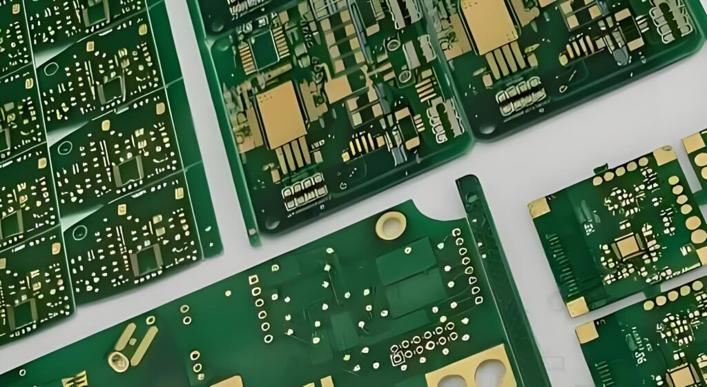
Overview of PCBA Manufacturing Process
The manufacturing of PCBA (Printed Circuit Board Assembly) is a crucial part of electronic product production. This process involves multiple precise steps, each of which significantly impacts the quality and functionality of the final product. The manufacturing process can be divided into three main parts: design and image transfer, printing and laminating, and assembly and testing.
1. Design and Image Transfer
The first step in PCBA manufacturing is creating the circuit design and transferring the images. Engineers design a schematic based on product requirements, which describes the connections between electrical components. Subsequently, the circuit design is accurately transferred onto blank PCBs using either laser direct imaging or traditional photographic techniques. Laser direct imaging technology offers higher accuracy and precision, ensuring the reliability of the circuit pattern and laying a solid foundation for the subsequent steps.
2. Printing and Laminating
Once the circuit pattern has been successfully transferred, the process moves on to the printing and etching stage. Engineers use chemicals to remove unwanted copper, forming the desired circuit pattern; this process requires great care to ensure the formation of a functional circuit. After etching, the layers of the PCB are bonded together through a laminating process, which not only ensures that electrical signals pass through the correct traces and components, preventing signal interference, but also enhances the overall structure and durability of the PCB, providing a reliable foundation for subsequent component installation.
3. Assembly and Testing
Finally, drilling and plating are key components of the PCB manufacturing process. Drilling is essential for mounting components and creating vias in multilayer PCBs, while plating provides a protective layer that prevents corrosion and environmental damage. During this phase, engineers assemble the circuit board, ensuring all electronic components are correctly connected through soldering or surface mount technology. Testing is a critical step to ensure that the PCBA operates correctly; through rigorous quality control, the final PCBA meets high standards of reliability and functionality.
Through this series of precise steps, PCBA manufacturing ensures high quality and efficiency in electronic products. The meticulous operation at each stage and the application of advanced technology ultimately drive the development of the electronics industry, enabling manufacturers to meet the growing market demands.
PCB Manufacturing Materials Overview
Selecting the right materials for PCB manufacturing is crucial for the performance and reliability of the final product. Different application scenarios and environmental requirements dictate the types of materials needed. Here are the primary materials commonly used in PCB manufacturing, along with their characteristics:
1. FR-4 (Glass-Reinforced Epoxy Laminate)
FR-4 is a widely used material in PCB manufacturing, known for its excellent electrical and mechanical properties. This material is waterproof and flame-retardant, making it suitable for high-temperature environments. Additionally, FR-4 offers high tensile strength and a favorable strength-to-weight ratio, making it the material of choice for standard and high-density PCBs. Its superior insulation properties ensure reliable circuit operation, which is why it is commonly used in consumer electronics, automotive, and industrial equipment.
2. PTFE (Polytetrafluoroethylene)
PTFE is a plastic with unique properties, particularly well-suited for high-speed, high-frequency, and high-power applications. This lightweight material provides excellent flexibility and temperature resistance, maintaining stable performance in harsh environments. PTFE does not produce any resistance, ensuring efficient signal transmission. As a result, it plays a critical role in microwave communications, aerospace, and medical devices.
3. Metal Materials (Copper, Aluminum, etc.)
Metal materials are widely used in PCB manufacturing due to their durability and strength, especially in applications that require resistance to high temperatures and harsh environments. Metals like copper and aluminum effectively dissipate heat, reducing the risk of overheating and enhancing the stability and longevity of the product. Moreover, these metals enable the application of Surface Mount Technology (SMT), allowing for the efficient integration of various components, thereby increasing the overall design flexibility.
When selecting materials for PCB manufacturing, it is essential to consider the specific needs of the product, environmental conditions, and any manufacturing constraints. By understanding the characteristics of different materials, engineers and designers can make informed decisions to ensure that the final product achieves optimal performance and reliability.
PCB Assembly Process

The PCB assembly process refers to the intricate steps involved in mounting electronic components onto a bare printed circuit board (PCB) after its manufacturing. This process is crucial for creating a fully functional PCB assembly (PCBA), and it comprises several key stages:
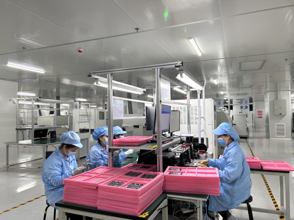
1. PCB Assembly Facility
The assembly begins in a specialized facility designed for efficient and precise operations. This area is equipped with advanced machinery and tools necessary for high-quality assembly.
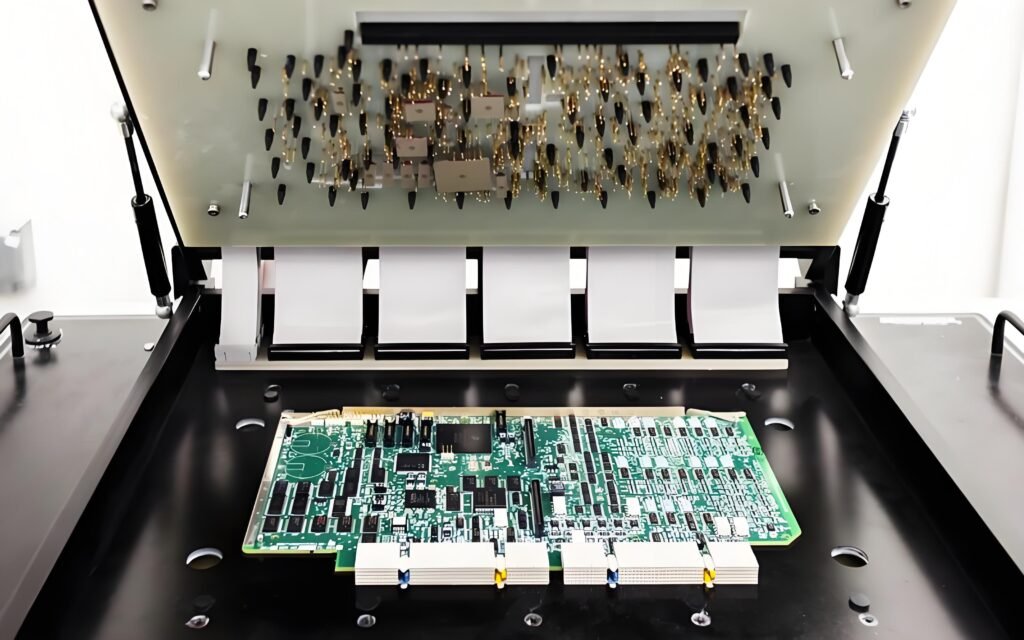
2. Pick and Place
During the pick-and-place stage, sophisticated machines employ Surface Mount Technology (SMT) to accurately position components onto the PCBA. This technology allows for the direct application of leadless components, particularly small ones, directly onto the surface of the circuit board, significantly enhancing efficiency. However, despite its advantages, SMT components are more susceptible to damage during installation, necessitating specialized soldering techniques and equipment to ensure proper handling and placement.
3. Through-Hole Component Insertion
For assemblies that include leaded components, through-hole insertion becomes essential. This process can be executed through manual soldering or wave soldering techniques. While manual soldering is often labor-intensive and time-consuming, wave soldering offers a more automated solution. However, wave soldering is not applicable to double-sided PCBAs. In cases where SMT is not feasible, through-hole insertion remains a highly effective option, ensuring secure connections for a variety of components.
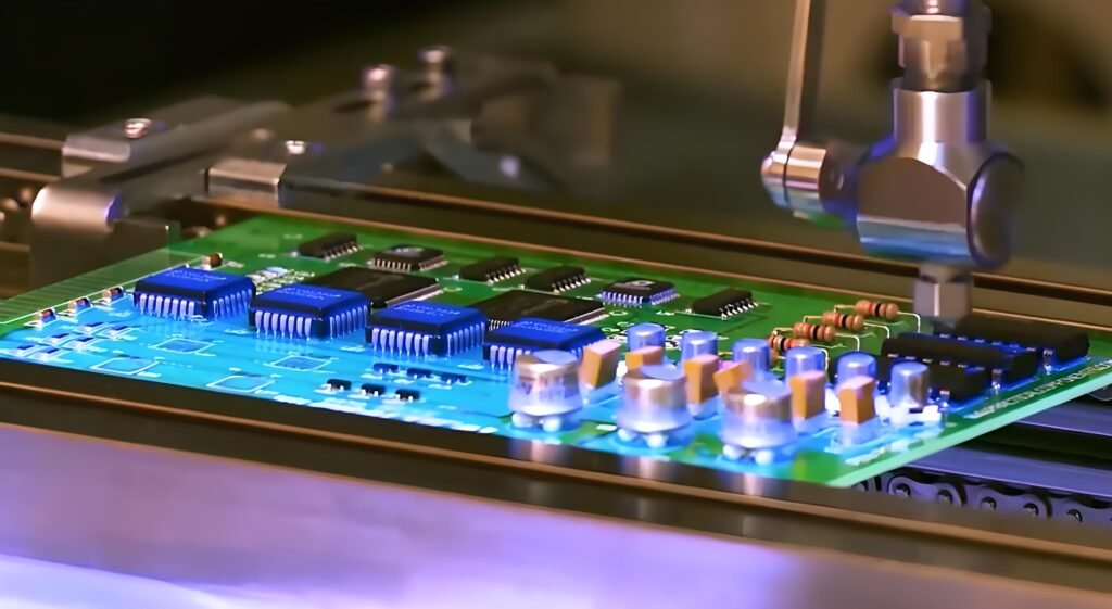
4. Reflow Soldering
After the components have been placed, the PCBA undergoes reflow soldering if SMT was used. The assembly is passed through a reflow oven, where the solder paste is melted, allowing it to adhere securely to the placed components. Following this, the PCBA moves through a cooling section where the solder solidifies, forming a permanent bond between the circuit board and the components. This step is critical for establishing reliable electrical connections that will endure throughout the product’s lifecycle.
5. Inspection and Quality Control
Once soldering is complete, a thorough inspection and testing phase is initiated. This step is vital, as it ensures that all connections are solid and that components are positioned correctly. Automated optical inspection (AOI) systems are often employed to detect defects such as solder bridges, misaligned components, and other issues that could compromise the assembly’s performance. This rigorous quality control process minimizes the risk of faults in the final product, ensuring that it meets both functional and regulatory standards.
The PCB assembly process is a complex yet essential phase in electronic manufacturing. Each step—from pick-and-place to inspection—plays a critical role in ensuring the reliability and functionality of the final product. By utilizing advanced techniques and rigorous quality control measures, manufacturers can produce high-quality PCBAs that meet the demands of today’s electronic applications.
PCBA Testing: Ensuring Quality and Reliability
PCBA testing is a critical component of successful electronic manufacturing. It plays a vital role in minimizing risks across various domains, ensuring that products are safe for consumers and meet established quality standards. Effective testing can significantly reduce returns associated with mass production issues and associated costs. Furthermore, it provides engineering teams with valuable insights to enhance their manufacturing processes for future projects.
Key Testing Considerations
When conducting PCBA testing, the following aspects should be thoroughly evaluated:
- Layer Quality: Ensuring maximum longevity for the PCBA by verifying the integrity of layers.
- Copper Quality: Assessing electrical conductivity and tensile strength to optimize performance.
- Solderability of Materials: Ensuring components are firmly attached to the circuit board to prevent failures.
- Hole Wall Quality: Checking for any cracking or delamination in the hole walls to maintain structural integrity.
- Leakage Current: Ensuring that current flows correctly throughout the circuit board without unintended paths.
- Environmental Durability: Testing the PCBA’s ability to withstand harsh environmental conditions.
- Cleanliness: Ensuring the PCBA is free from contaminants that could lead to corrosion and failure.
Common Testing Methods
Several effective testing methods are employed to evaluate PCBA quality, including:
- In-Circuit Testing (ICT): One of the most common methods due to its speed and efficiency. In this process, a fixture with numerous sensor points is aligned with specific functions on the PCB. As the board passes through, the fixture quickly contacts the board to identify any non-functional points.
- Flying Probe Testing: This method does not require fixtures. Instead, the PCB is held in place while testing probes move to contact specific points. Although more customizable, flying probe testing is generally slower than ICT. However, it allows engineers to swiftly adjust test points using software.
- Functional Testing: This method focuses on ensuring that the entire PCBA operates as intended. Conducted during the final stages of manufacturing, products are rated based on pass/fail criteria to confirm their operational reliability.
- Boundary Scan Testing: Particularly useful for multilayer and high-density PCBAs, this method allows engineers to test connections on the PCB when traditional testing methods are inadequate due to inaccessible nodes.
The Importance of Process Testing
Process testing refers to evaluations conducted at various stages throughout the manufacturing process. Engineering teams will assess different components and circuit boards during the PCBA manufacturing and assembly phases. This testing can take various forms, ranging from visual inspections to electrical and functional tests.
Process testing is crucial for early detection of potential issues that could escalate into more significant problems later in production. Identifying defects, errors, or inconsistencies early on helps ensure the final product meets quality and performance expectations.
In addition to enhancing the quality of the final product, process testing can save significant time and money. By promptly addressing any issues, manufacturers can avoid costly delays and rework that may arise later in the manufacturing process. This proactive approach also minimizes the risk of product recalls or returns, which can be expensive and detrimental to brand reputation.
In summary, PCBA testing is essential for guaranteeing the quality and reliability of electronic products. By implementing thorough testing strategies throughout the manufacturing process, companies can ensure that their products meet consumer safety standards and operate effectively in their intended applications. This not only safeguards the brand’s reputation but also enhances customer satisfaction and loyalty.
Quality Control in PCBA Manufacturing
Quality control in PCBA manufacturing is essential for ensuring that products are safe, reliable, and effectively meet their intended purposes. It encompasses a wide range of activities aimed at identifying defects before the products reach consumers. The testing procedures discussed earlier are integral to the overall quality control framework.
Key Quality Control Activities
Effective quality control involves several inspection and verification methods, including:
- Visual and Microscopic Inspections: These inspections involve trained personnel, often those involved in assembly, examining the PCBA either with the naked eye or through a microscope. This method is crucial for spotting visible defects such as misaligned components or soldering issues.
- X-Ray Inspection: X-ray technology enables engineers to identify defects in the circuit board that might not be visible during standard inspections. This includes issues like solder bridges and hidden component defects, which can significantly impact performance.
- Automated Optical Inspection (AOI): AOI systems capture images of the PCBA and compare them against a reference image of the ideal board configuration. Any discrepancies highlighted by the system indicate potential defects that require further investigation, allowing for quick corrective actions.
- Design Rule Check (DRC): DRC is a critical process that verifies the schematic against manufacturing capabilities. It helps ensure that designs are feasible and compliant with manufacturing constraints, preventing teams from proceeding with designs that could lead to production challenges.
Enhancing Quality Control Processes
To bolster quality control efforts, manufacturers can adopt additional practices:
- Statistical Process Control (SPC): Utilizing statistical methods to monitor and control the manufacturing process can help identify trends or variations that may indicate quality issues, allowing for timely interventions.
- Failure Mode and Effects Analysis (FMEA): Implementing FMEA allows teams to systematically evaluate potential failure modes of a product and their causes, prioritizing them based on their impact and likelihood. This proactive approach facilitates the development of strategies to mitigate risks.
- Regular Audits and Reviews: Conducting frequent quality audits and process reviews helps ensure compliance with established standards and fosters a culture of continuous improvement within the organization.
- Employee Training and Engagement: Investing in training programs for employees involved in quality control can significantly enhance their ability to identify and address potential issues. Engaged employees are more likely to take ownership of quality and contribute to a robust quality culture.
In conclusion, quality control in PCBA manufacturing is a multifaceted approach that plays a pivotal role in ensuring product reliability and safety. By employing a variety of inspection methods and continuous improvement strategies, manufacturers can effectively mitigate defects and enhance overall product quality, ultimately leading to greater customer satisfaction and trust in their products.
Learn More About the PCBA Manufacturing Process
PCBA manufacturing is a complex and systematic process that encompasses multiple stages from design to quality control. Each phase is crucial, as various errors can occur during manufacturing and assembly. Therefore, it is essential to have a comprehensive understanding of each stage and its associated tools.
Importance of the Design Stage
The design of PCBA must not only be flexible but also take into full consideration the key elements of manufacturing, assembly, and testing. It is essential to integrate manufacturability and testability into the design to ensure the product’s feasibility and efficiency in actual production. This means that designers should closely collaborate with the manufacturing team to ensure that the design can be effectively translated into a producible product.
Material Selection and Manufacturing Technologies
Choosing the right materials is critical in PCB manufacturing. In addition to traditional materials, modern manufacturing should also consider utilizing advanced imaging technologies, such as laser direct imaging, to enhance precision and reliability. These technologies can ensure the clarity of circuit patterns, reduce defect rates during the production process, and consequently improve the quality of the final product.
Advantages of Automated Assembly
The PCB assembly phase should heavily rely on automated equipment to minimize human errors and increase production efficiency. Automation not only accelerates production speed but also enhances assembly accuracy, ensuring that components are correctly placed. By employing advanced Surface Mount Technology (SMT) and robotic assembly lines, companies can achieve efficient and consistent production.
The global electronic product manufacturing market is projected to reach $800 billion. To maintain a competitive edge in this intense market environment, companies must optimize all aspects of PCBA manufacturing and assembly to meet the growing global demand. By enhancing design flexibility, selecting appropriate materials, implementing automation, and strengthening testing and quality control, businesses will be able to improve product quality and market competitiveness, thereby driving sustainable development.
