Comprehensive Guide to Printed Circuit Board Testing Methods
For any designer, the worst nightmare is discovering product flaws at the final stage. Despite careful design and manufacturing, all types of electronic products, including Printed Circuit Boards (PCBs), are susceptible to issues. Many problems surface during the prototyping phase, often requiring troubleshooting and adjustments. However, uncovering issues only after a product has been launched can lead to costly consequences for a company.
PCB testing plays a crucial role in preventing these issues. Given the complexity of PCBs and their central role in electronic devices, thorough testing is essential to ensure performance, reliability, and quality. In this guide, we will delve into the significance of PCB testing and explore the key methods used to evaluate and verify the functionality of PCB designs.
Why PCB Testing Is Essential for Quality and Reliability
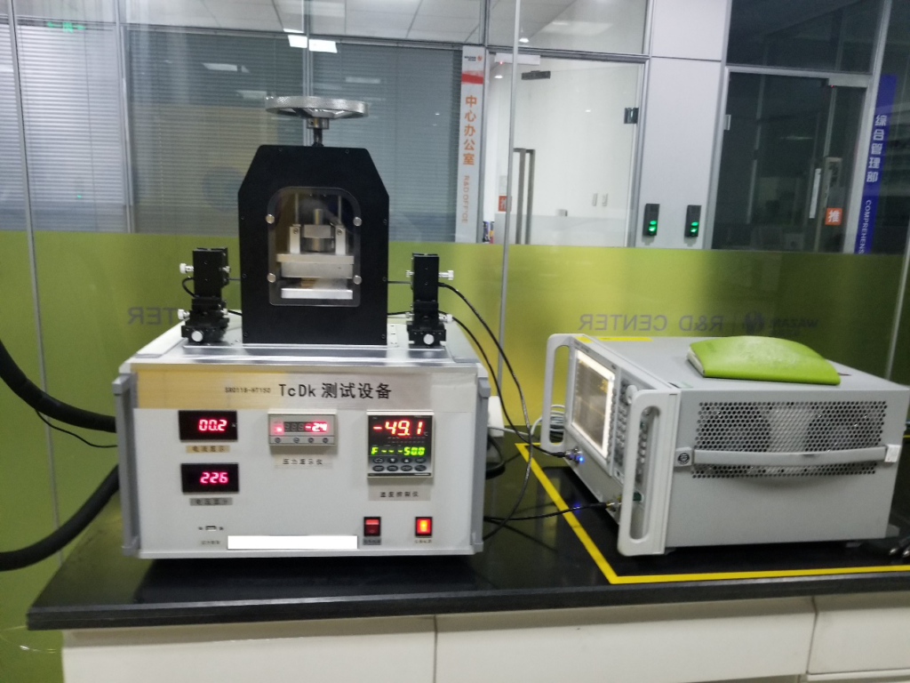
Testing is an integral part of the PCB manufacturing process. Conducting tests throughout the production cycle helps minimize risks and avoid costly issues in the final stages of production. While design analysis techniques can be employed early on to mitigate potential manufacturing problems, PCB testing methods are crucial for identifying defects in physical circuit boards. These tests, often conducted on prototypes or small batches, focus on detecting issues such as short circuits, faulty solder joints, and functionality discrepancies to ensure that each PCB meets its intended performance standards.
The Key Benefits of PCB Testing
For many companies, PCB testing is not just a precaution but a vital step in the design and production process. The advantages of thorough PCB testing extend beyond just identifying faults—they significantly impact production efficiency, cost savings, and long-term product reliability. Here’s why PCB testing is indispensable:
- Fault Detection and Issue Identification
The primary benefit of PCB testing is its ability to pinpoint problems early in the design and manufacturing process. Whether the issue lies in functionality, manufacturability, or layout design, PCB tests provide critical insights into potential flaws, allowing designers to make necessary adjustments before production moves forward. By detecting these issues at an early stage, the likelihood of costly redesigns or product recalls is significantly reduced. - Time Efficiency
Early-stage PCB testing saves valuable time by helping designers identify major issues early in the prototype phase. Comprehensive testing enables designers to quickly diagnose root causes of problems and make adjustments, which accelerates the production process. This, in turn, helps shorten time-to-market, ensuring that products are delivered to customers faster, thereby enhancing business agility and competitiveness. - Cost Reduction
PCB testing, particularly during the prototype or small-scale production phase, helps avoid costly mistakes. By thoroughly testing designs before mass production, companies can ensure that only fully functional and manufacturable PCBs move to production. This minimizes the risk of waste associated with defective PCBs, ultimately reducing material and labor costs. Early detection of faults prevents the need for expensive rework or the production of unusable units, ensuring cost-effective manufacturing. - Reduced Return Rates and Customer Complaints
Implementing rigorous PCB testing minimizes the likelihood of selling defective products, which can lead to costly returns, repairs, and customer dissatisfaction. By ensuring that PCBs meet performance standards before they reach the consumer, businesses can significantly reduce the volume of returns and warranty claims. This not only improves the bottom line by reducing operational costs but also enhances brand reputation and customer loyalty. - Enhanced Safety Standards
Since PCBs are often integral to critical electronic systems, their failure can have severe consequences, including potential safety hazards. A malfunctioning PCB can lead to fire risks, electrical malfunctions, or even cause equipment failure in high-stakes industries such as healthcare, aerospace, and automotive. Pre-production testing guarantees that the final product adheres to safety regulations and prevents failures that could jeopardize personnel or operations.
While not all PCBs require extensive testing, particularly for mature products that have already gone through rigorous validation, new PCB designs demand robust and frequent testing to ensure optimal performance and safety. By establishing a comprehensive testing protocol tailored to your company’s needs, you can unlock the full benefits of PCB testing, ultimately improving product quality, reducing costs, and enhancing overall customer satisfaction.
In conclusion, implementing thorough PCB testing is an investment in the future success of your product line. Whether you’re refining prototypes or scaling up production, ensuring the quality and reliability of your PCBs is essential to delivering high-performance, safe, and cost-effective products.
Understanding PCB Testing: What Is Tested and Why It Matters
PCB testing is a critical step in ensuring the quality, reliability, and functionality of printed circuit boards (PCBs). During the PCB manufacturing process, various testing methods are employed to verify that the PCB meets the required specifications and standards, ensuring it performs as intended without defects. These tests cover a wide range of physical and electrical checks, which help detect potential issues early in the production cycle. In this guide, we will explore the key components of PCB testing and the critical factors evaluated during the testing process.
Key Components Tested in PCB Evaluation
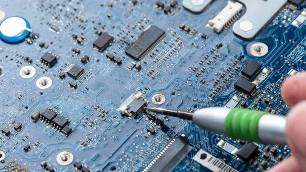
PCB testing involves a comprehensive evaluation of several key components of the board. Each of these components is subjected to rigorous testing to ensure it performs correctly and adheres to industry standards. Below are the major components and aspects that are commonly tested during the PCB evaluation process:
- Lamination Quality
The lamination process is fundamental to the integrity and lifespan of a PCB. If the laminate delaminates (separates from the board), it can lead to circuit failure. Lamination testing assesses the board’s resistance to delamination under stress or heat. The test ensures that the board can withstand mechanical and thermal forces without compromising its structure, which is vital for the overall reliability of the PCB. - Copper Plating
Copper foil is an essential conductive layer on the PCB, and its quality directly impacts the performance of the circuit. Copper plating tests evaluate the copper’s adhesive strength, tensile strength, and elongation rate. These tests ensure that the copper layers are properly bonded to the board and can withstand the mechanical stresses encountered during operation. Additionally, the uniformity of copper plating is tested to ensure consistent conductivity across the board. - Solderability
Solderability tests are crucial for ensuring that components can be effectively soldered onto the PCB without issues. This is particularly important for preventing defects like poor solder joints, which could lead to failure in the final product. The primary focus of solderability testing is “wetting”—the ability of the surface to accept molten solder. This test is conducted by analyzing the PCB’s ability to maintain reliable solder joints, which are critical for the functionality of the final assembly. - Hole Wall Integrity
The quality of the hole walls in a PCB is another vital component. Any cracks or delamination in the hole walls can affect the PCB’s mechanical and electrical performance. Testing the hole walls involves evaluating their resistance to cracking or peeling, particularly under thermal stress. This is typically done through temperature cycling or by exposing the PCB to rapid changes in environmental conditions to ensure the holes retain their integrity. - Electrical Conductivity
Electrical conductivity is a key test for any PCB, as it directly impacts the board’s performance. This test ensures that the PCB has minimal leakage when current passes through its conductive traces. Conductivity tests help to identify any short circuits or open circuits that could cause malfunctions or failure of the board. The goal is to verify that the electrical paths are intact and capable of supporting the intended load without excess resistance. - Environmental Resistance
Many PCBs are used in environments with high humidity, temperature fluctuations, or exposure to corrosive substances. To simulate real-world conditions, environmental tests are conducted to assess the board’s durability under these conditions. One common test is water absorption, where the PCB’s weight is measured before and after exposure to a humid environment. A significant weight change indicates the PCB’s susceptibility to moisture damage, which can lead to corrosion or degradation of electrical properties. - Cleanliness and Corrosion Resistance
The cleanliness of a PCB is vital for its long-term reliability. Contaminants, dirt, or residues left on the PCB can lead to corrosion or electrical shorting. Cleanliness tests typically assess the PCB’s resistance to corrosion when exposed to various environmental stressors like moisture, temperature extremes, and pollutants. These tests ensure that the PCB can function optimally in harsh environments and will not fail due to environmental exposure. - Functional Testing
After the individual components are tested for their physical properties, functional testing is carried out to ensure the PCB operates as intended. Functional tests simulate the electrical behavior of the board in real-world conditions, checking for any irregularities in performance, such as voltage irregularities, signal integrity issues, or component malfunctions. This test validates that the PCB performs its intended function without failure.
The Importance of PCB Testing
The purpose of PCB testing is to identify potential issues early in the manufacturing process, which helps reduce the risk of product failure, minimizes waste, and ensures that the final product meets performance standards. Early detection of defects allows for cost-effective corrections before mass production begins, saving both time and money. For high-stakes applications—such as medical devices, aerospace, and automotive electronics—rigorous PCB testing is essential to ensuring safety, reliability, and compliance with industry standards.
By implementing a thorough and comprehensive PCB testing process, manufacturers can ensure that their boards are capable of withstanding mechanical stress, electrical loads, and environmental conditions. In addition, it helps companies minimize the risk of costly recalls, reduce return rates, and enhance customer satisfaction by delivering high-quality products.
In conclusion, PCB testing is an essential step in the electronics manufacturing process. By employing a range of testing methods to evaluate key components of the PCB, manufacturers can ensure that their boards are not only functional but also durable and reliable. This comprehensive approach to testing ultimately leads to better product quality, reduced costs, and improved performance, making it an indispensable part of PCB production.
Types of PCB Testing Methods: A Comprehensive Guide
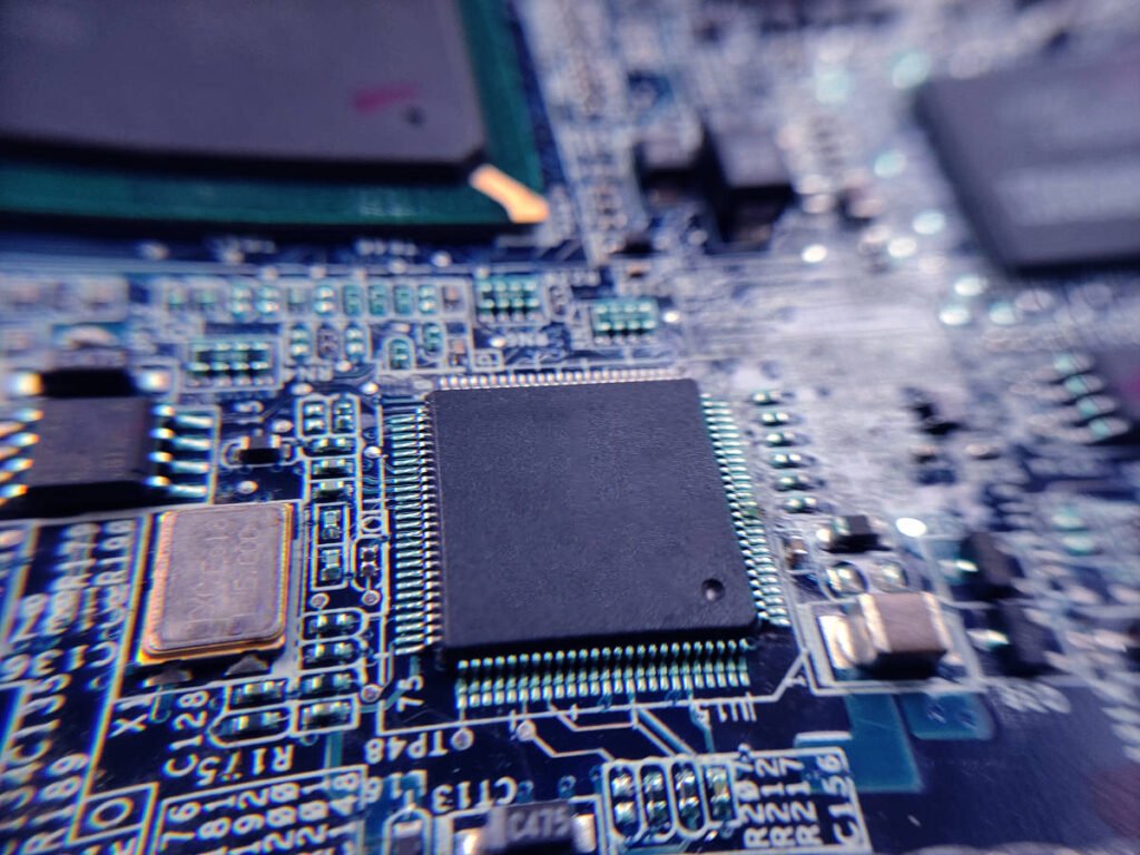
PCB testing is an integral part of the manufacturing process, ensuring that printed circuit boards (PCBs) are functional, reliable, and free of defects. Different testing methods are used to assess the quality of the PCB based on its design and intended application. Choosing the right testing method depends on several factors, including the type of PCB being tested, the issues being investigated, and the overall production environment.
In this guide, we explore the most common PCB testing methods, detailing their advantages, limitations, and appropriate use cases. These four popular methods are widely employed in the industry to ensure that PCBs meet the necessary performance standards.
1. In-Circuit Testing (ICT)
In-Circuit Testing (ICT) is one of the most widely used and effective testing methods in the PCB industry. It offers high accuracy and is capable of detecting up to 98% of PCB faults, making it an essential tool for identifying defects early in the production process. ICT tests individual components and their connections on the PCB, without needing to power the entire board.
How it Works:
ICT utilizes a test fixture that connects to a network of sensors or “test pins,” which make contact with various points on the PCB. These points are monitored and measured to verify that they meet expected parameters. The key components of an ICT system include:
- Test Fixture: A custom-designed fixture that securely holds the PCB during testing. The fixture is equipped with a grid of test pins that make contact with specific test points on the PCB.
- Test Instrumentation: A series of diagnostic devices, such as oscilloscopes and multimeters, connected to the test fixture to measure electrical properties like resistance, capacitance, and inductance.
- Software: A program that defines the test parameters, communicates with the test equipment, and interprets the results. The software also helps determine whether the tested PCB passes or fails the test.
Advantages of ICT:
- High Accuracy: ICT is highly effective in detecting faults, such as open circuits, short circuits, and component failure.
- Suitable for Mass Production: This method is best suited for high-volume production runs where the cost of setting up the test fixture can be justified.
- Comprehensive Testing: ICT can test both individual components and the overall integrity of the PCB.
Limitations:
- High Setup Costs: The cost of the test fixtures and equipment can be significant, making ICT most suitable for large-scale production.
- Limited for Complex Designs: It is less effective for testing complex, high-density designs where many nodes are inaccessible.
2. Flying Probe Testing (FICT)
Flying Probe Testing, also known as Fixtureless In-Circuit Testing (FICT) or Flying Needle Testing, is a versatile and cost-effective testing method that eliminates the need for custom test fixtures. This method uses a set of movable probes or needles to make contact with test points on the PCB, as controlled by software.
How it Works:
In FICT, the test probes are mounted on a set of motors that move the probes across the PCB to specific test points. The probes test components and connections individually, similar to ICT but without the need for a fixed test fixture. The probes are controlled via software that directs them to perform electrical tests.
Advantages of FICT:
- No Custom Fixtures Required: This significantly reduces the initial setup cost, making FICT ideal for low-to-medium volume production and prototyping.
- Flexibility: FICT can easily accommodate design changes with minimal adjustments to the test program.
- Quick Setup: The lack of a custom fixture speeds up the setup process, making it a good option for fast-turnaround projects.
Limitations:
- Slower Than ICT: While FICT is flexible, it is generally slower than ICT due to the time required for the probes to move to different test points.
- Less Suitable for Large-Scale Production: For high-volume production, FICT may not offer the same throughput as ICT, making it less efficient for mass manufacturing.
3. Functional Testing
Functional Testing is typically performed at the end of the PCB production process and focuses on ensuring that the PCB performs according to its design specifications. This test simulates the operating environment of the finished PCB and verifies that it functions as intended under real-world conditions.
How it Works:
Functional testing involves using a functional test system that connects to the PCB to simulate its intended operational conditions. The PCB is powered up, and its functionality is evaluated by measuring key performance indicators such as voltage, current, and signal integrity. Functional testers often use edge connectors or probes to interact with the PCB.
Advantages of Functional Testing:
- Final Verification: This test confirms that the PCB operates correctly as a complete system, ensuring that the design works as intended.
- Ideal for Complex Systems: Functional testing is especially effective for more complex or customized PCBs that may not be adequately tested using simpler methods like ICT or FICT.
- Real-World Simulation: It provides a real-world simulation of the PCB’s actual use, offering insights into potential issues that may arise during normal operation.
Limitations:
- Not for Early Stages: Functional testing is typically performed at the end of the production cycle, making it unsuitable for early-stage defect detection or design validation.
- Cost and Complexity: Functional testing systems can be expensive and complex to set up, particularly for designs with a large number of variables.
4. Boundary Scan Testing
Boundary Scan Testing is a specialized method that is particularly useful for high-density, multi-layer PCBs, where access to internal nodes is difficult or impossible. This method utilizes the built-in test circuitry of integrated circuits (ICs) to perform a comprehensive test of the PCB without physical contact.
How it Works:
Boundary scan testing works by using a method called IEEE 1149.1 (commonly known as JTAG). This method leverages test points embedded within the ICs and connects these points to a test access port. Using a boundary scan controller, the system can test the connectivity and functionality of components without needing to access every node directly.
Advantages of Boundary Scan Testing:
- Non-Intrusive: Since no physical contact is required with the PCB, this method is ideal for multi-layer and highly compact PCBs.
- Effective for High-Density Circuits: It is particularly useful for testing modern, high-density designs that are difficult to probe with traditional methods.
- Fast and Comprehensive: Boundary scan can quickly identify faults in complex circuits and is widely used for system-level testing.
Limitations:
- Requires Support from Components: Not all components support boundary scan testing, so this method is best used with ICs that include built-in test circuitry.
- Limited to Digital Circuits: Boundary scan is best suited for digital circuits and may not be effective for analog components or high-frequency signals.
How to Protect Your PCB Through Better Design

In modern electronics design and manufacturing, ensuring the reliability and high quality of PCBs (Printed Circuit Boards) is critical. By utilizing some of today’s top design practices early in the design phase, you can significantly improve the manufacturability, assemblability, testability, and supply chain stability of your PCB, reducing manufacturing issues, lowering costs, and extending product lifecycle performance. Below are some key design methodologies that will help you avoid common problems during manufacturing and improve the overall quality of your PCB.
1. Design for Manufacturability (DFM)
Design for Manufacturability (DFM) focuses on arranging PCB topology with manufacturing constraints in mind. This design approach aims to address common issues encountered during the manufacturing and assembly process, ensuring the PCB is easy to fabricate and free of common design flaws.
Key Considerations:
- Floating Copper & Islands: Free-floating copper areas or islands on a PCB layer can lead to issues during production, especially during the etching process. These areas might cause interference, inaccurate trace impedance, or other defects. DFM design should avoid complex circuit regions with small islands or floating copper.
- Solder Bridges: When traces and pads are placed too close to each other, and no solder mask is used, solder bridges can form, causing short circuits or other electrical issues. DFM ensures proper trace spacing and adequate solder mask coverage to prevent solder bridges.
- Copper-to-Edge Issues: If copper traces are too close to the edge of the PCB, they can cause short circuits during the etching process. DFM requires maintaining a safe distance between copper areas and the board’s edges to avoid production issues.
Benefits of DFM:
- Improves manufacturability by addressing potential issues early.
- Reduces defect rates and rework costs.
- Identifies manufacturing challenges before production begins, saving time and costs.
2. Design for Assembly (DFA)
Design for Assembly (DFA) focuses on designing PCBs that are easy to assemble, ensuring that components can be securely attached to the board during the assembly process. A poorly designed PCB can make assembly challenging, so DFA ensures that the design facilitates fast, efficient assembly.
Key Considerations:
- Material Simplification: Minimize the number of materials and components used in the design to simplify the assembly process.
- Component Selection: Choose widely available, standardized components to reduce sourcing difficulties and avoid rare or complex parts.
- Spacing Between Components: Ensure adequate spacing between components to allow easy handling and placement during assembly, minimizing the risk of assembly errors.
- Clear Marking: Ensure that all component labels and markings are clear and easy to interpret, so assembly staff can identify parts quickly and accurately.
Benefits of DFA:
- Reduces assembly complexity and time.
- Lowers labor costs and improves assembly efficiency.
- Prevents potential assembly problems and delays caused by poor design.
3. Design for Testability (DFT)
Design for Testability (DFT) ensures that the PCB is designed in a way that facilitates thorough, efficient testing during production. A DFT approach makes it easier to detect and troubleshoot faults, speeding up the test process and improving the accuracy of fault detection.
Key Considerations:
- Ease of Fault Diagnosis: Design the PCB so that every component and circuit node can be easily tested. Make it straightforward to isolate faults in the circuit for quick troubleshooting.
- Test Point Layout: Ensure that the PCB has sufficient test points and connectors for using various testing methods, such as In-Circuit Testing (ICT) or Functional Testing.
- Accessibility: For multi-layer or high-density PCBs, ensure that inner layers can be tested using non-contact methods like boundary scan or X-ray.
Benefits of DFT:
- Makes fault detection more efficient, reducing debugging time.
- Accelerates the testing process, reducing time to market.
- Minimizes the risk of shipping faulty boards, improving product quality and customer satisfaction.
4. Design for Supply Chain (DFSC)
Design for Supply Chain (DFSC) involves considering the long-term availability of components and their lifecycle during the PCB design process. This methodology ensures that the selected components can be reliably sourced throughout the PCB’s product lifecycle, avoiding issues related to component obsolescence and supply shortages.
Key Considerations:
- Component Lifecycle Management: Design with the knowledge of the lifecycle of components, ensuring that they remain available for the duration of the PCB’s lifecycle. Avoid components that are likely to be discontinued during the product’s lifecycle.
- Alternative Parts Selection: Collaborate with experienced contract manufacturers early in the design phase to identify and select components that are easy to source and have available alternatives if required.
- Supply Chain Transparency: Work closely with suppliers to ensure they can provide the components required for the design, and maintain sufficient inventory levels to avoid supply chain disruptions.
Benefits of DFSC:
- Ensures long-term availability of components, reducing the risk of supply chain issues.
- Extends the lifecycle of the PCB design, ensuring the product remains viable for a longer period.
- Reduces costs and production delays caused by obsolete or out-of-stock components.
By adopting Design for Manufacturability (DFM), Design for Assembly (DFA), Design for Testability (DFT), and Design for Supply Chain (DFSC) methodologies, PCB designers can mitigate common design flaws and manufacturing issues. These practices ensure that the PCB can be easily manufactured, assembled, tested, and sourced, resulting in lower production costs, reduced time to market, and improved overall product quality. Effective design not only enhances the performance of the PCB but also extends its lifecycle, contributing to the long-term success and competitiveness of the product.
Choose CustomPCBA for PCB Testing
PCB testing is a critical step in the design and manufacturing process, enabling companies to catch potential issues before they impact production. By identifying and addressing design flaws early, businesses can save substantial time and money. However, to ensure accurate and efficient testing of your PCBs, partnering with a reliable supplier is essential. That’s where CustomPCBA comes in.
We specialize in providing high-quality PCB prototyping and small-batch production services, streamlining the testing process and accelerating your project timelines. Our team is dedicated to delivering consistent and reliable prototypes, ensuring your boards are produced exactly as per your specifications, every time. With a commitment to transparency and no hidden fees, we offer you the confidence you need to move forward with your PCB testing, knowing that your prototypes are in capable hands.
Trust CustomPCBA to deliver high-quality, precision-manufactured PCBs that meet the demands of your testing phase, enabling you to efficiently progress to the next stage of your project. Get in touch today for a fast, competitive quote and take the next step toward successful PCB testing!

