Printed Circuit Boards (PCBs) form the backbone of modern electronic devices. They serve as the essential platform that transmits electrical signals between interconnected electronic components, enabling them to function properly.
For any electronic device or system to operate effectively, it requires high-quality PCBs. As technology advances, consumer expectations for electronics are becoming more demanding. Manufacturers can gain a competitive edge by understanding the intricacies of PCB manufacturing processes. With an increasing number of organizations engaging in PCB production, the global PCB market is projected to reach $107.6 billion by 2030, underscoring the critical role of PCBs in the evolving electronics industry.
How Are Circuit Boards Manufactured?
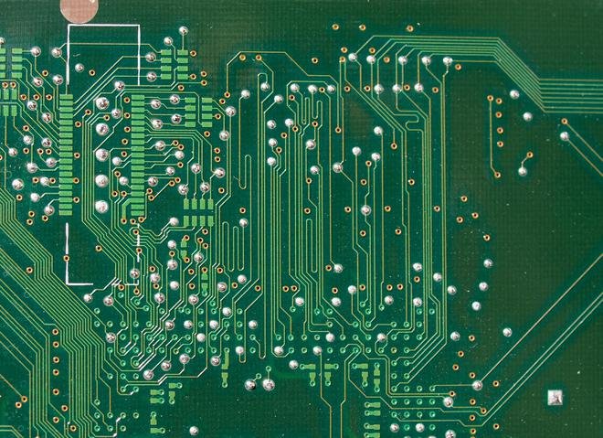
A Printed Circuit Board (PCB) is a non-conductive material upon which conductive traces (also known as tracks or traces) are printed or etched. Electronic components are mounted on the PCB, and these traces interconnect the components to form functional circuits. PCBs provide both physical and mechanical support for the majority of electronic devices, ensuring proper electrical connectivity and integration.
The industrial manufacturing process of PCBs involves multiple stages, checks, and balancing steps to ensure that the final product meets the required performance specifications. The structure of PCBs can vary, being single-sided, double-sided, or multi-layered, with differences in structure only occurring after the first layer is completed. The complexity of the PCB core can also vary, and many PCBs may require upwards of 20 manufacturing steps to be fully realized.
Types of Printed Circuit Board Designs
PCB designs are categorized based on design specifications, manufacturing techniques, and the intended application. Below are the most commonly used types of PCBs:
Single-Sided PCB
The single-sided PCB is the most basic type of PCB. It consists of a single layer of conductive copper on one side of a non-conductive substrate. Electronic components are placed on one side of the board, while the etched circuit traces are visible on the opposite side. Due to the limitation of only having one conductive layer, the traces cannot overlap, which can sometimes result in a larger design footprint.
Single-sided PCBs are ideal for low-density designs and are often used in basic, cost-effective electronic devices. These boards are easy to design, manufacture, and maintain.
Double-Sided PCB
Double-sided PCBs feature a conductive layer on both the top and bottom surfaces of the board. Holes drilled into the board allow traces and component leads to pass through, connecting the two sides. Manufacturers use various mounting methods to connect the circuits on both sides of the PCB.
Double-sided PCBs offer several advantages, including reduced size, compact circuits, and higher density, making them suitable for advanced electronic systems at a relatively low cost. These boards can support more complex designs than single-sided ones and are widely used in modern electronics.
Multi-Layer PCB
Multi-layer PCBs consist of two or more layers of copper. These layers are sandwiched between insulating material, creating a layered structure. High pressure and temperature are used to bond the layers together, ensuring stable PCB components and eliminating any voids or air gaps.
These boards are designed to be compact and offer higher flexibility in terms of complexity, making them ideal for high-speed applications. Multi-layer PCBs allow for much higher circuit densities and greater routing options, which is particularly important for modern electronics with advanced functionality.
Rigid PCB
A rigid PCB has a solid substrate material that gives the board rigidity and strength, preventing warping or bending. These PCBs are composed of several layers, which typically include:
- Substrate material (often fiberglass)
- Copper layers for conductive traces
- Solder mask to protect the traces
- Silkscreen layer for component placement and identification
The layers are bonded together using adhesives and heat. Rigid PCBs are durable and easy to diagnose and repair. Their robust construction makes them well-suited for a wide range of applications, from medical devices to consumer electronics such as laptops.
Flexible PCB
Flexible PCBs are constructed with multiple layers of printed circuits and components on a flexible substrate, such as polyimide, PEEK (Polyetheretherketone), or clear conductive polyester film. The design of these PCBs allows them to be bent or flexed during installation, offering a significant advantage in applications where space is limited or flexibility is required.
Flexible PCBs are available in single-sided, double-sided, and multi-layer configurations. Aside from their flexibility, these boards are compact, highly reliable, and capable of withstanding repeated flexing, making them ideal for applications requiring high signal density and reliability, such as in wearable devices, automotive electronics, and high-performance communications systems.
The History of PCB Manufacturing

The concept of the Printed Circuit Board (PCB) dates back to 1903 when German inventor Albert Hanson filed the first patent for a basic PCB design, followed by more advanced patents for complex variations. Over the past century, the PCB industry has witnessed monumental progress, particularly in the last fifty years, enabling enhanced functionality at the microscopic level, significantly boosting the performance of compact devices.
The military played a pivotal role in transforming PCB manufacturing. The U.S. Army Signal Corps developed automated assembly techniques to accelerate PCB production, making it more efficient and cost-effective for mass production in consumer electronics.
In the last five decades, we have advanced to producing multi-functional, lightweight PCBs, allowing consumers to experience various media types within a single device. As we enter a new age of innovation, PCBs will continue to serve as the backbone of technological advancements—from autonomous vehicles to smart homes.
Key Components of a PCB

A Printed Circuit Board (PCB) is composed of four fundamental layers that are critical to its structure and function:
- Substrate: The substrate is typically made from fiberglass or other composite materials. It forms the core framework of the PCB, providing mechanical strength and preventing breakage. It acts as the skeleton of the PCB, offering stability and structural integrity under stress and during thermal fluctuations.
- Copper Layer: The copper layer is crucial for conducting electrical signals within the PCB. It can either be in the form of copper foil or a complete copper coating, depending on the type of PCB. This layer serves as the conductive pathway for electrical signals, functioning similarly to the human nervous system by transmitting information between components.
- Solder Mask: The solder mask is a polymer coating applied to the PCB to protect the copper traces from oxidation, accidental short circuits, and the ingress of solder in undesired locations. This layer helps ensure the PCB’s electrical integrity during the manufacturing process and is critical for preventing damage and performance issues. However, it is not used as an electrical insulator.
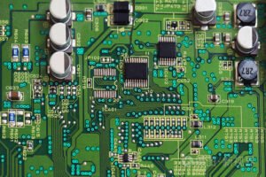
- Silkscreen: Often referred to as the legend or markings, the silkscreen layer provides vital information such as component identifiers, switch settings, test points, and other notations. It is typically printed on the component side of the PCB to guide assembly, troubleshooting, and maintenance.
Each of these components contributes to the functionality and reliability of the PCB, ensuring that it serves its role as a critical foundation in electronic devices.
How Are PCBs Made?
The steps of the PCB design process start with design and verification and continue through the fabrication of the circuit boards. Many steps require computer guidance and machine-driven tools to ensure accuracy and prevent short circuits or incomplete circuits. The completed boards must undergo strict testing before they are packaged and delivered to customers.
1. PCB Design
The first step in PCB manufacturing is designing the circuit using Electronic Design Automation (EDA) software such as Altium Designer, KiCad, etc. The circuit design forms the foundation of the PCB, where the designer selects components, traces, and ensures the design meets electrical, mechanical, and thermal requirements. This stage also involves considering factors like current carrying capacity, signal integrity, and impedance matching.
2. DFM (Design for Manufacturability) Check
The DFM check ensures the design is manufacturable and avoids potential production issues. This includes checking minimum trace width, minimum spacing, hole sizes, and layer stack-up. A DFM review helps identify design flaws, such as inadequate trace widths or overly small holes, which could cause problems during manufacturing.
3. Printing the Circuit Diagram
After completing the design, the files are converted into Gerber files and used to create photomasks for transferring the circuit patterns onto the PCB. This process is referred to as “printing,” as it involves transferring the circuit design patterns onto the PCB using photolithography. These printed patterns are the blueprint for the manufacturing process.
4. Photolithography and Exposure
The next step involves applying a photosensitive layer (photoresist) to the PCB, which is then exposed to ultraviolet (UV) light through a photomask. The exposed areas harden, while the unexposed portions remain soft. These unexposed portions are later removed through a developing process, creating the circuit patterns on the board.
5. Etching
After photolithography, the remaining copper that is not covered by the photoresist is etched away using a chemical solution (such as ferric chloride). This leaves behind the copper traces that form the circuit pattern on the PCB. The etching process must be precise to avoid removing unwanted copper or leaving unclean edges.
6. Cleaning and De-resisting
Once the etching is complete, the photoresist (used during the photolithography step) must be removed. This is done using a chemical solvent to clean the board and expose the copper traces. The PCB is then thoroughly cleaned to ensure no resist residues remain, as these could affect the performance of the board.
7. Drilling
Drilling is performed to create holes in the PCB for component leads or vias (electrical connections between layers). These holes are drilled precisely using CNC machines. Accurate hole size and placement are crucial, particularly for high-density PCBs, as the hole-to-pad alignment and diameters must be controlled tightly.
8. Plating
Plating involves electroplating a thin layer of copper onto the walls of drilled holes, creating electrical connections between the top and bottom layers of the PCB. Plating enhances conductivity and allows for multilayer circuit boards to function properly by ensuring electrical continuity through vias.
9. Outer Layer Imaging and Etching
For double-sided or multilayer PCBs, the outer layers of the board must also go through imaging and etching. Similar to the inner layers, the outer layers are imaged with photolithography and then etched to create the required traces. This step ensures that the top and bottom of the PCB contain the necessary circuit patterns.
10. Solder Mask Application
A solder mask (usually green) is applied to protect the copper traces on the PCB and prevent oxidation. It also helps protect the PCB during the soldering process, ensuring that only the pads where components will be soldered are exposed. The solder mask is applied using photolithography and develops into a protective layer over the PCB.
11. Silkscreen Printing
Silkscreen printing is used to print text and symbols onto the surface of the PCB, such as component labels, logos, and electrical connection identifiers. A screen-printed stencil is used to apply ink to the PCB in a precise manner. This step helps identify component locations and aids assembly and troubleshooting.
12. Electrical Testing
After the PCB is fabricated, electrical testing ensures that the board functions correctly. Common methods include Flying Probe Testing and Automated Optical Inspection (AOI). Flying Probe Testing checks for shorts, opens, and correct connections. AOI checks for errors in the board’s copper traces and soldering quality.
13. Cutting and Depaneling
Once the PCB is complete, it is typically part of a larger panel that contains multiple boards. Depaneling involves cutting the large PCB panel into individual units. This is done either by mechanical cutting or laser cutting, ensuring precise cuts that follow the edge of the board without damaging the circuit.
14. Surface Finishing
Surface finishing processes are applied to enhance the board’s solderability, corrosion resistance, and electrical performance. Common surface finishes include Hot Air Solder Leveling (HASL), lead-free soldering, and immersion gold. The surface finish chosen depends on the application, environmental conditions, and soldering requirements.
15. Packaging and Delivery
After final inspection and testing, the PCBs are packaged to protect them from static and physical damage during transportation. Common packaging materials include anti-static bags, foam, or other cushioning materials. The packaged boards are then delivered to the customer or sent for further assembly.
16. Soldering
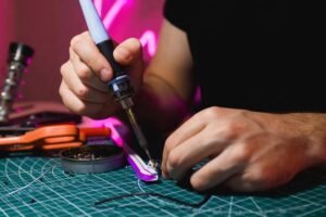
Soldering is the process of attaching electronic components to the PCB using a soldering technique. For through-hole components, this can involve hand soldering or wave soldering, while surface-mount devices (SMD) typically use reflow soldering. Proper control of temperature and solder material is necessary to avoid damage to the components or PCB.
17. Assembly
After soldering, components are fully assembled onto the PCB. Surface-mount components are typically placed using automated pick-and-place machines, while through-hole components are inserted manually or via machines. Proper component orientation and placement are essential for the board’s functionality.
18. Re-testing
Once assembled, the PCB undergoes a series of functional and electrical tests to ensure it works as expected. This may involve both manual testing and automated test equipment (ATE). The goal is to verify that all components are correctly placed and that the board is free of faults such as short circuits or faulty connections.
19. Debugging and Optimization
In this stage, any issues that arise during testing are resolved. This could involve adjusting the design or making minor modifications to the PCB or components. Debugging ensures that the board functions optimally in its intended application, and this phase is critical for high-performance or complex designs.
20. Customer Acceptance
Before final delivery, the PCB is subjected to customer acceptance testing, where the customer reviews the board for defects, performance, and adherence to specifications. Once the board passes this final inspection, it is accepted, and production can proceed for larger quantities, if needed.
How to Implement an Effective PCB Manufacturing Process
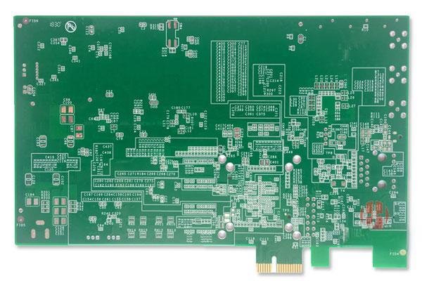
PCB (Printed Circuit Board) manufacturing is a complex process that typically involves various teams and collaborators. In many cases, a Contract Manufacturer (CM) may assemble the PCB with components based on the design created by the Original Equipment Manufacturer (OEM). Ensuring an efficient process requires close collaboration between these teams, particularly in areas such as component selection, design considerations, file formats, and materials. Effective cooperation across departments and organizations is crucial for a seamless transition between each stage of the manufacturing process.
1. Design for Manufacturability (DFM) Considerations
Design for Manufacturability (DFM) is a critical step that ensures the PCB design can be efficiently translated into a physical product during manufacturing. The core objective of DFM is to optimize the design to make sure it can be produced without issues in the manufacturing process. Designers should work closely with manufacturers to understand the capabilities and limitations of the manufacturing plant to ensure the design complies with production requirements.
Manufacturers typically provide a set of DFM guidelines that OEM design teams can refer to when optimizing their designs. By adhering to these manufacturing standards early in the design phase, designers can avoid production delays or quality issues that may arise from poor design choices. Additionally, designers should collaborate with manufacturers on material availability, ensuring the selected materials are compatible with existing production capabilities while meeting design specifications.
2. Material Selection and Coordination
Selecting the appropriate materials is a crucial step in PCB design. Designers need to work with manufacturers to determine which board materials and components should be used, ensuring that these materials meet design specifications while also providing cost-effective solutions. In some cases, OEMs may specify more expensive materials that the PCB manufacturer does not typically use, which could lead to delays or higher costs. Designers and manufacturers must collaborate to select materials that balance design requirements with cost-efficiency.
Material coordination goes beyond just selecting the right raw materials; it also involves considering the manufacturer’s production capabilities and supply chain reliability. If certain components or materials are unavailable, the design team and manufacturer must come to a consensus on alternative solutions to prevent manufacturing delays while still meeting the design’s functional and performance requirements.
3. Unified File Formats
PCB design files serve as the primary means of communication between the OEM and the PCB manufacturer. To avoid errors or data loss that may arise from format inconsistencies, both the OEM and the manufacturer must use compatible file formats. The most commonly used file formats in the PCB industry are Gerber and IPC-2581, as they ensure that design files can be transferred smoothly between different software and systems.
Moreover, the design files should include comprehensive annotations and instructions, particularly for complex multilayer boards, fine-pitch components, or specific material requirements. Standardized file formats not only improve production efficiency but also reduce the risk of misunderstandings between the design team and the manufacturer regarding the design’s intent.
4. Communication and Coordination with Manufacturers
Effective communication between the OEM and PCB manufacturer is critical for ensuring the design and production phases are aligned. In addition to technical documentation and material requirements, designers should regularly communicate with manufacturers to discuss project progress, address any production issues, and resolve design changes. Ongoing communication helps identify potential bottlenecks or conflicts early, allowing for timely solutions that prevent rework or delays.
By collaboratively addressing material shortages, production limitations, or other issues, the design and manufacturing teams can work together to ensure the PCB is produced as specified. Regular feedback and coordination help avoid unnecessary complications and ensure the product meets the quality and functional requirements.
5. Balancing Cost-Effectiveness and Quality
When selecting materials and finalizing designs with manufacturers, cost-effectiveness and quality are two critical factors that need to be balanced. Designers should fully understand how the choice of materials and manufacturing techniques will impact the cost and work towards optimizing the design to minimize unnecessary expenses while maintaining the desired quality.
At the same time, manufacturers should offer solutions that improve production efficiency, reduce unit costs, and shorten the overall lead time. A well-executed DFM strategy can help ensure that the design is functional, manufacturable, and cost-effective. This balance of quality and cost is essential for achieving competitive production cycles without compromising product integrity.
Why Choose Us?
Since 2005, CustomPCBA has been a trusted provider of bare printed circuit boards (PCBs) to a wide range of customers. Over the past two decades, we have built lasting relationships with clients across various industries, ranging from small startups to large enterprises. Our commitment to customer satisfaction remains at the forefront of everything we do, offering rapid response times, flexible delivery schedules, and comprehensive technical support.
From our inception, we have focused on redefining the standard for customer service while streamlining our internal processes to meet the evolving demands of the industry. We ensure that your PCBs are manufactured to meet relevant industry standards while maintaining competitive pricing and the highest quality, helping you achieve both efficiency and profitability in your projects.

