The Importance of PCB Trace Width Calculators

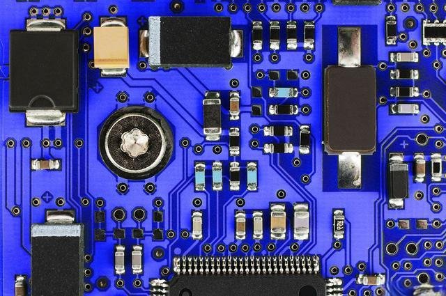
Printed Circuit Boards (PCBs) are integral to nearly all modern electronic devices. Whether you're working with medical equipment, lighting systems, or consumer electronics, PCBs provide mechanical support and electrical connectivity for components to ensure the proper functioning of the device. One of the key aspects of designing an effective PCB is ensuring that trace widths are calculated correctly.
Using a trace width calculator ensures that the PCB traces are not only wide enough to carry the required current but also designed to prevent overheating, excessive power loss, and potential damage to the board. In this article, we'll explore why calculating trace width is essential, and how trace width calculators can help you design PCBs that are safe and efficient.
Why Use a Trace Width Calculator?

A trace width calculator is a tool that helps you determine the ideal width for a PCB trace based on parameters such as the amount of current the trace needs to carry, temperature rise, and the type of copper used in the PCB. This calculation is crucial because it ensures that traces can handle the required electrical load without overheating or causing performance issues.
If the traces are too narrow, they may overheat, leading to reduced conductivity, or even failure of the PCB. On the other hand, if the traces are too wide, the PCB layout may become unnecessarily large, increasing the cost and complexity of manufacturing. A trace width calculator enables designers to find the optimal trace width that strikes a balance between safety, performance, and cost-effectiveness.
What Does a PCB Trace Width Calculator Do?
The trace width calculator works by using established formulas to calculate key parameters that determine the width of the traces on the PCB. The main parameters it helps calculate include:
- Maximum Current Capacity: The calculator helps determine the maximum current that can safely flow through the trace without exceeding the temperature limits for the material.
- Trace Resistance: This calculation estimates the resistance of the trace, which is essential for ensuring efficient power transmission and preventing excessive heat generation.
- Voltage Drop: The calculator can estimate the voltage drop across the trace due to its resistance and the amount of current flowing through it.
- Power Dissipation: This refers to the amount of power lost as heat in the trace, which is a key consideration for maintaining the thermal stability of the PCB.
Key Calculations for PCB Trace Width
Here’s an overview of the formulas used by a typical trace width calculator:
Maximum Current Calculation
The formula for calculating the maximum current capacity is:
[
I_{\text{MAX}} = \frac{(k \times T_{\text{RISE}} \times b)}{A} \times c
]
Where:
- I_MAX = Maximum current (Amperes)
- T_RISE = Maximum allowable temperature rise (°C)
- k, b, c = Constants depending on the copper type and other materials
- A = Trace cross-sectional area
Temperature Rise Calculation
The trace temperature is a critical factor when calculating trace width to avoid overheating. The formula is:
[
T_{\text{TEMP}} = T_{\text{RISE}} + T_{\text{AMB}}
]
Where:
- T_TEMP = Final trace temperature (°C)
- T_RISE = Expected temperature rise due to current flow (°C)
- T_AMB = Ambient temperature (°C)
Resistance Calculation
To determine the resistance of the trace, the following formula is applied:
[
R = \frac{ \rho \times L}{A'} \times \left(1 + \alpha \times (T_{\text{TEMP}} - 25°C)\right)
]
Where:
- R = Trace resistance (Ohms)
- ρ = Resistivity of copper (Ω·cm)
- L = Length of the trace (cm)
- A' = Cross-sectional area of the trace (cm²)
- α = Temperature coefficient of resistance (1/°C)
- T_TEMP = Trace temperature (°C)
Voltage Drop Calculation
The voltage drop across a PCB trace is a measure of energy loss and is calculated as:
[
V_{\text{DROP}} = I \times R
]
Where:
- V_DROP = Voltage drop (Volts)
- I = Current (Amperes)
- R = Trace resistance (Ohms)
Power Dissipation Calculation
To estimate how much heat a trace will generate, the following formula for power dissipation is used:
[
P_{\text{LOSS}} = R \times I^2
]
Where:
- P_LOSS = Power loss (Watts)
- R = Resistance of the trace (Ohms)
- I = Current (Amperes)
Common Questions About Trace Width Calculators
For those who are new to using trace width calculators, the process can seem daunting. Here are some common questions and answers to help clarify how to use the tool and interpret the results:
What is a mil?
- A "mil" is a unit of measurement commonly used in PCB design, equal to 1/1000th of an inch. This unit is often used for trace width and spacing measurements.
What does temperature rise mean?
- Temperature rise refers to the increase in temperature of the PCB trace when current flows through it. It is the difference between the maximum operating temperature and the ambient temperature.
Does the calculator have limitations?
- Yes, the calculator may have certain limitations based on the formulas used, such as a maximum allowable trace width (400 mils), maximum current (35 Amps), and copper thickness range (0.5-3 oz/ft²). When these limits are exceeded, the calculator may extrapolate the data.
Why are internal traces often wider than external traces?
- Internal traces in multi-layer PCBs generally have less effective heat dissipation than external traces because they are surrounded by other layers. Therefore, internal traces need to be wider to prevent excessive heating.
Conclusion
Using a trace width calculator is an essential step in designing a reliable and safe PCB. By accurately calculating trace widths, designers can ensure that the PCB can handle the required electrical current, minimize power loss, and avoid overheating. This tool helps avoid design flaws, reduces the risk of failures, and ensures that the board performs optimally throughout its lifecycle.
Whether you are working on a simple consumer product or a high-performance industrial application, leveraging a trace width calculator will improve the efficiency, reliability, and longevity of your PCB designs.


