Reverse engineering plays a critical role across various industries, particularly for those working with Printed Circuit Boards (PCBs). By employing PCB reverse engineering, you can gain valuable insights into the board's functionality and design, which can be crucial for tasks such as repair, upgrading outdated circuit boards, or even producing cost-effective alternatives that outperform competitors. Understanding how to reverse engineer a PCB offers a deeper comprehension of its operational mechanics, and the process itself brings numerous advantages.
In this article, we will explore the concept of reverse engineering, outline the benefits it offers for your PCBs, and provide a step-by-step guide on how to successfully reverse engineer a PCB to maximize its potential.
What Does PCB Reverse Engineering Involve?
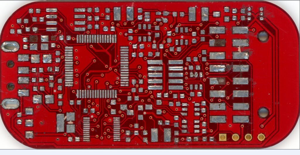
PCB reverse engineering is a comprehensive and systematic process that includes targeted PCB analysis, reverse analysis, and the replication of PCB design techniques. This method is crucial for identifying and extracting key functional and structural design features, as well as manufacturing processes of a product. By gathering this information, companies can develop products with similar functionalities and capabilities, all while ensuring they do not create an exact replica of the original reverse-engineered PCB.
Reverse engineering is primarily employed to understand and deconstruct the underlying design principles of a product. This approach is particularly valuable when the design information for a specific product is not readily available or accessible.
The most common method of PCB reverse engineering involves disassembling a sample PCB for detailed examination. Based on this analysis, companies create comprehensive documentation outlining the product’s design methodology and operational characteristics. This documentation typically includes in-depth details regarding the design approach, component placement, and electrical functions of the board.
Using the insights gained from the sample PCB, companies can then produce a similar board that may outperform the original or competitor products in terms of performance, cost-efficiency, or overall functionality. Beyond simply analyzing and surpassing competitors’ products, PCB reverse engineering enables companies to improve their own designs. By identifying outdated components, security vulnerabilities, or design flaws, businesses can enhance the functionality and reliability of their PCBs, thus optimizing the end product’s performance and longevity.
Benefits of PCB Reverse Engineering
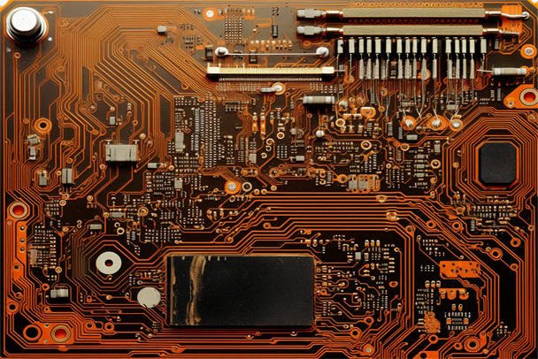
PCB reverse engineering offers numerous advantages, making it an invaluable tool for companies across various industries. Whether you are working with outdated PCBs, troubleshooting undocumented designs, or seeking to outperform competitors, reverse engineering provides actionable insights that can significantly improve product development and operational efficiency. Below are some of the key benefits of PCB reverse engineering:
1. Maintenance of Critical Legacy PCBs
In many industries, legacy PCBs play a crucial role in powering machinery or electronic components. Over time, these boards may become obsolete or no longer supported by the original manufacturer, making repairs or replacements challenging. Reverse engineering outdated PCBs enables companies to replicate these critical components, ensuring continued operation even when original parts are no longer available. This approach also provides a means to create spare parts or replacements when a board is beyond repair, effectively extending the lifespan of essential equipment.
2. Extracting Information from Undocumented PCBs
While modern PCBs are typically accompanied by documentation or CAD files, many older or third-party boards lack such supporting materials. In these cases, reverse engineering becomes an essential process for extracting critical schematic and design information. By disassembling and analyzing these boards, engineers can reconstruct the necessary documentation, which serves as a valuable resource for troubleshooting, maintenance, or replication. This process not only fills in the gaps but also allows businesses to fully understand the functionality and design of a given PCB.
3. Reducing Dependence on External Experts
When a PCB malfunctions or is difficult to repair, companies often rely on specialized engineers or external experts for diagnostics and troubleshooting. However, the lack of readily available expertise can pose a significant challenge, particularly if the PCB is rare or complex. Reverse engineering enables in-house teams to acquire the necessary information to identify and address issues independently. By understanding the design and functionality of the PCB, internal teams can efficiently detect potential failure points and resolve problems without relying on costly external specialists.
4. Identifying Weaknesses in Competitor Designs
For companies in the PCB manufacturing industry, reverse engineering competitors’ designs offers valuable insights into potential weaknesses or inefficiencies in their products. By analyzing competitor PCBs, businesses can pinpoint areas for improvement, such as design flaws, component selection, or manufacturing techniques. Armed with this knowledge, companies can refine their own designs to offer more efficient, cost-effective, or feature-rich products. This competitive edge can lead to stronger market positioning, improved customer satisfaction, and increased sales, even if the goal isn’t to directly compete in the same market segment.
5. Reducing Production Costs
High manufacturing costs are often a barrier to entry in the PCB market, particularly when competitors are able to command a premium price for their products. Reverse engineering allows companies to gain a clear understanding of the actual cost structure behind a competitor’s PCB. By identifying the materials, components, and production processes used, companies can find ways to optimize their own manufacturing methods and reduce costs. This cost-saving advantage enables businesses to produce similar or superior PCBs at a lower price point, offering a more competitive product while attracting price-sensitive customers who may not have had viable alternatives.
6. Enhancing Design Innovation
Reverse engineering also fosters design innovation by allowing engineers to explore alternative approaches to existing solutions. By understanding the fundamental workings of a competitor's PCB, businesses can experiment with different materials, layouts, and technologies to improve functionality, efficiency, or performance. This process not only leads to better products but also encourages a culture of continuous improvement and innovation within the organization.
How to Perform PCB Reverse Engineering
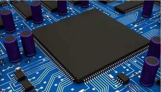
Performing PCB reverse engineering is a complex and time-consuming process, but the benefits it offers in terms of understanding and improving circuit board design are invaluable. This process allows you to replicate, repair, or optimize PCBs, potentially creating more efficient or cost-effective alternatives. The process involves several key stages, each requiring specialized knowledge and tools. Below is a detailed breakdown of how to perform PCB reverse engineering:
1. Prepare the PCB Images: Drawing, Scanning, or Photographing
The first step in reverse engineering a PCB is to acquire high-quality images of the board. This can be done through drawing, scanning, or photographing the PCB.
- Photography and Scanning: When photographing the PCB, ensure you capture both sides of the board and use a dark-colored background to minimize interference from copper pads. Using a high-resolution camera or smartphone is essential, and ensuring good lighting is key to capturing detailed images. This step can also involve extensive post-processing, such as adjusting brightness and contrast, to enhance visibility.
- Manual Layout Drawing: For simpler PCBs, you may opt to manually draw the layout on graph paper, ensuring accuracy in scale and using standard symbols for components. Although manual drawing can be labor-intensive, it can bypass some of the more complex editing processes required for digital images.
2. Upload and Process the Image
Once you have captured or scanned the PCB images, the next step is to upload them to reverse engineering software for further processing. Before uploading, it is advisable to crop the images to remove any irrelevant background or borders.
- Image Editing Software: Common image editing tools include GIMP, Inkscape, and AutoTrace. These open-source, free tools allow you to edit and enhance the images for better clarity. GIMP and Inkscape can help with cleaning up the image, adjusting colors and contrasts, while AutoTrace is used to convert bitmap images into vector graphics, which can then be used to create more accurate PCB layouts.
3. Build the PCB Layout
After uploading the images into reverse engineering software, the next step is to construct the PCB’s 3D layout. This layout represents the board's electromagnetic field distribution, component placements, and the wiring arrangement across layers.
- Editing and Adjustments: For simple PCBs, tools like AutoTrace can quickly convert bitmap images to vector graphics, providing a good starting point for creating the layout. For more complex PCBs, you may need to spend additional time editing the image to ensure accuracy in translating the layout. Some common adjustments include:
- Painting Pads and Holes: Before processing the PCB, "paint" the pads and holes to ensure they are not lost in the conversion process. This can be done by swapping channels to improve visibility.
- Removing PCB Touchpads: For programs like AutoTrace, it is necessary to remove any touchpads or test pads from the PCB image, as they may create unwanted loops in the conversion process.
- Marking Unconnected Holes: In multilayer boards, there are often holes or regions that are not connected to any other part of the board. These should be clearly marked during the editing stage for easy identification.
- Adjusting Saturation and Layering: Increase the visibility of the PCB’s details by adjusting the saturation and the number of layers, especially for multilayer designs.
- Cleaning Tracks: Clean up the tracks on the PCB to ensure they are not cluttered before converting the image. Clear tracks will result in better layout accuracy and clearer schematics.
4. Create the Schematic Diagram
The next step is to create a schematic diagram, which is a critical part of PCB reverse engineering. A schematic shows how all the components on the PCB are interconnected and how the board functions.
- Exporting the Schematic: Once the layout is finalized, export the schematic using CAD software like AutoTrace, Target 3001!, or similar PCB layout tools. This step is typically easier than layout construction, as most of the image editing is already complete. The schematic will provide a 2D representation of the board’s electrical design, which is essential for understanding the PCB’s operation and troubleshooting.
- Labeling and Organizing: Ensure that all components are properly labeled and that the tracks are arranged logically in the schematic. This will make it easier to understand the connections between components and troubleshoot issues.
5. Integrating Both Sides of the PCB Layout
To complete the reverse engineering process, you need to combine the layouts of both sides of the PCB. This step is essential for creating a comprehensive two-sided schematic that represents the full design of the PCB, particularly for multilayer boards.
- Combining and Aligning: Once the layouts of both sides are completed, ensure that all components are properly aligned and all tracks are clearly represented. This will allow you to visualize the full PCB design, making it easier to repair or replicate the board.
6. Troubleshooting and Optimization
After completing the layout and schematic, you now have a complete understanding of how the PCB works. At this point, you can troubleshoot any issues or make improvements to the design.
- Repair and Optimization: If the goal of reverse engineering is to repair the PCB, use the schematic to identify faulty components or broken connections. If you are optimizing the design, you can identify areas where performance could be improved, such as reducing component size, optimizing routing, or improving power distribution.
Conclusion
By following these detailed steps, you can effectively reverse engineer a PCB and gain a thorough understanding of its design and functionality. While the process requires time and expertise, it offers tremendous value for engineers and manufacturers who need to replicate, repair, or improve circuit boards. With the right tools and techniques, PCB reverse engineering provides deep insights into a design, enabling you to enhance your product’s performance, reliability, and efficiency.

