Printed Circuit Board Testing: Ensuring Quality and Reliability in Electronics Manufacturing
Testing is a critical step in the Printed Circuit Board Assembly (PCBA) manufacturing process, playing a vital role in identifying and resolving potential issues before the product reaches the consumer. This step ensures both the functionality and integrity of the product, which directly impacts customer satisfaction and reliability. However, with the numerous testing methods available, selecting the optimal approach for a given project can be challenging. Below is an overview of the most common PCB testing methods, outlining their advantages, limitations, and ideal applications.
1. Visual Inspection (VI)
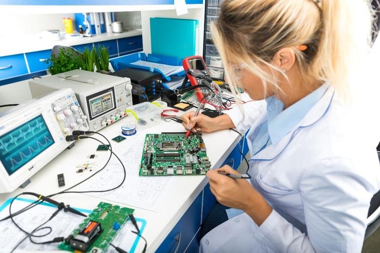
Visual inspection is typically the first line of defense in the testing process. It involves checking the PCBA for defects using the naked eye, magnifying tools, or Automated Optical Inspection (AOI) systems. The AOI system uses high-resolution cameras and software to detect common defects such as component misalignment, solder bridges, or missing/damaged parts.
Advantages:
- Quick and cost-effective.
- Capable of identifying surface-level defects like misaligned components, solder bridges, and missing parts.
Limitations:
- May miss defects that are not visible to the naked eye or hidden beneath components.
- Limited in detecting internal issues like circuit path malfunctions or deeper electrical faults.
Best for:
- Identifying gross defects in PCBs during high-volume production.
- Screening for visual issues such as component placement or soldering problems.
2. In-Circuit Testing (ICT)
In-Circuit Testing (ICT) is one of the most widely used methods for testing PCBs during production. It involves the use of specialized test fixtures, or “bed-of-nails,” that make electrical contact with designated test points on the PCBA. ICT measures various electrical properties such as resistance, capacitance, and inductance to detect issues like open circuits, short circuits, or incorrect component values.
Advantages:
- Provides high test coverage and accuracy.
- Can detect a wide range of electrical faults.
Limitations:
- Requires the development of custom test fixtures for each specific design, which can be time-consuming and costly.
- Not as flexible for prototype or low-volume production.
Best for:
- High-volume production environments where precision and comprehensive testing are required.
- Applications where high accuracy is crucial, such as safety-critical electronics.
3. Flying Probe Testing (FPT)
Flying Probe Testing (FPT) is a non-contact testing method that uses a set of movable probes to electrically contact the test points on the PCBA. These probes systematically test each point in a predefined sequence. Unlike ICT, FPT does not require custom fixtures, making it a flexible and cost-effective solution for low-to-medium volume production and prototyping.
Advantages:
- More flexible and cost-effective than ICT, especially for low-volume or prototype production.
- No need for custom test fixtures.
Limitations:
- Slower than ICT, which can lead to longer testing times.
- May not provide the same level of test coverage as ICT.
Best for:
- Prototyping or small-batch production where flexibility is required.
- Shorter test runs where customization of test fixtures is not feasible.
4. Functional Circuit Testing (FCT)

Functional Circuit Testing (FCT) is used to assess the overall functionality of the PCBA by simulating the actual operating conditions of the final product. This involves applying power and input signals to the board and measuring the output responses to verify that the board functions as intended. FCT can identify performance-related faults such as issues with signal processing, power supply, and timing errors.
Advantages:
- Tests the board under conditions similar to real-world use, ensuring the functionality of the entire system.
- Can identify performance-related faults that other methods might miss.
Limitations:
- Requires the development of custom test setups, which can be time-consuming and expensive.
- May not pinpoint the exact location of faults, making troubleshooting more difficult.
Best for:
- Verifying the functionality of the PCBA after it has been assembled.
- Ensuring the final product operates as expected in a simulated end-user environment.
5. Boundary Scan (JTAG)
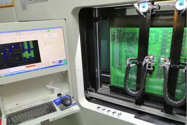
Boundary Scan, also known as JTAG (Joint Test Action Group), is a method that uses the built-in test circuitry within the components of a PCB to perform tests on the board. The components in the PCB are connected to form a “boundary scan chain,” allowing the test equipment to directly assess the functionality of each component and its interconnections.
Advantages:
- Excellent for testing high-density boards or boards with limited physical access.
- Provides high test coverage and can identify faults that other methods cannot.
Limitations:
- Requires components with built-in boundary scan capabilities, which may not be present in all designs.
- Setup and configuration of JTAG testing can be complex and time-consuming.
Best for:
- Testing high-density or complex PCBs where other methods may not be practical.
- Situations where physical access to the board is restricted, such as in multi-layer or high-density designs.
6. Automated Optical Inspection (AOI)
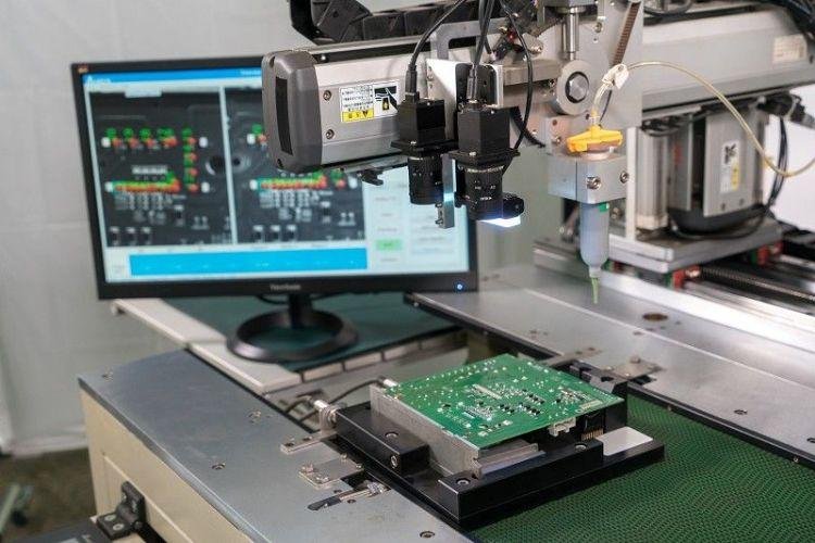
Automated Optical Inspection (AOI) is an advanced visual inspection method that uses high-resolution cameras and computer algorithms to automatically detect defects in the PCBA. AOI systems are equipped with sophisticated software that can compare the actual assembly to a known good reference and identify anomalies such as component misplacement, soldering issues, or other visual defects.
Advantages:
- Fast and efficient, capable of inspecting large volumes of boards quickly.
- Can detect a wide range of surface-level defects and is highly accurate.
Limitations:
- Limited to surface-level defect detection; cannot detect internal circuit faults.
- May miss defects hidden beneath components or those that are not visible to the camera.
Best for:
- High-volume production where speed and efficiency are crucial.
- Surface-level inspections such as soldering defects and component alignment.
7. X-Ray Inspection
X-Ray Inspection is used primarily for testing multi-layer or complex PCBs, where internal defects such as solder voids, hidden cracks, or misalignments cannot be detected with optical inspection methods. The system uses X-ray technology to scan the internal layers of the PCB, providing detailed images of the internal structure.
Advantages:
- Can detect internal defects such as solder voids, misalignments, and cracks.
- Non-destructive and highly accurate for complex PCBs.
Limitations:
- Expensive and often used only for high-end or specialized products.
- Requires specialized equipment and expertise.
Best for:
- Multi-layer PCBs or complex designs with hidden internal layers.
- High-value or critical applications where internal defects cannot be overlooked.
Choosing the Right Testing Method
Selecting the most appropriate PCB testing method depends on various factors such as project requirements, production volume, budget, and time constraints. Below are some key considerations:
- Project Requirements:
- Assess the complexity of the PCB design and the potential risks associated with defects. If your PCB involves high-density or multi-layer designs, consider methods like JTAG or X-ray for thorough inspection.
- Production Volume:
- For high-volume production, In-Circuit Testing (ICT) is often preferred due to its high accuracy and comprehensive test coverage. For small batches or prototypes, Flying Probe Testing (FPT) or Automated Optical Inspection (AOI) might be more practical.
- Budget:
- Evaluate the cost of each testing method, including setup, equipment, and maintenance. While ICT and JTAG offer high test coverage, they can also incur significant upfront costs, making them less feasible for low-budget projects.
- Test Accessibility:
- Consider the physical layout and design of the PCBA. For high-density boards with restricted access, boundary scan (JTAG) or X-ray inspection might be necessary.
- Turnaround Time:
- Some testing methods, such as ICT, may take longer due to the need for custom fixtures. In contrast, methods like AOI and FPT offer faster turnaround times, making them ideal for time-sensitive projects.
Conclusion
A comprehensive testing strategy is essential to ensure the quality and reliability of PCBs in electronics manufacturing. By selecting the appropriate testing methods based on the design complexity, production volume, and budget, manufacturers can effectively detect and resolve potential issues early in the production process. Balancing cost and testing coverage is key to achieving high-quality, reliable PCBs that meet both functional and performance standards. As the electronics industry continues to evolve, incorporating advanced testing technologies will remain crucial in optimizing production efficiency and product quality.

