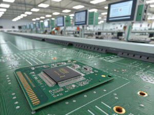
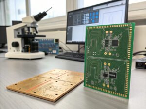
In the manufacturing of printed circuit boards (PCBs), both the bare board and the bare board testing process play critical roles. The bare board layout serves as the foundation for the placement of vias and electronic components, shaping the overall structure of the PCB. Additionally, the printed circuitry on this substrate defines the connectivity of the finished board. By incorporating bare board testing into the PCB development process, engineers can significantly enhance the reliability and functionality of the final product, ensuring that the circuit design performs as intended. This process is essential for identifying potential issues early in the design phase, ultimately leading to higher-quality PCBs and more efficient production workflows.
Understanding Bare PCBs: The Foundation of Circuit Board Manufacturing
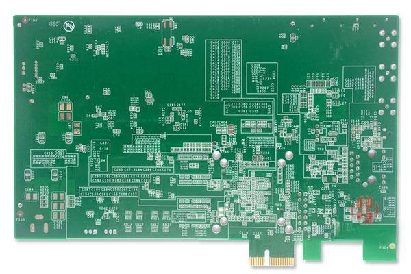
In PCB (Printed Circuit Board) terminology, a "bare board" refers to the initial stage of the PCB before any components, such as resistors, capacitors, or integrated circuits, are soldered onto it. It consists of the base substrate material, conductive copper traces, and vias, which are the essential elements that allow the board to function as a medium for electrical connections. The bare board is essentially the framework of the PCB, featuring its metallic layers, insulation, and the intricate conductive pathways designed during the layout process.
The substrate material of a bare board is typically made from fiberglass (e.g., FR4), which is durable and provides mechanical support, along with electrical insulation. Over this substrate, copper layers are deposited or etched to form the conductive traces that will later carry electrical signals. These traces are carefully designed to route power, data, and ground connections throughout the circuit.
In industry, a distinction is often made between a "bare board" and a "Printed Circuit Board Assembly" (PCBA). The bare board is the precursor to the fully assembled circuit board, which includes the soldering of electronic components into place. While the bare board is a critical part of the PCB manufacturing process, it alone does not perform any function until components are added and connected to the circuit.
Additionally, the quality of the bare board is essential to the overall performance and reliability of the final product. Factors such as trace width, via design, layer stack-up, and impedance control are crucial during the design of a bare board to ensure the PCB can handle the electrical and thermal demands of the final device. Consequently, bare board testing — such as electrical continuity and isolation checks — is a vital step to confirm that the board meets the required specifications before the assembly phase begins.
In summary, the bare board serves as the foundation of the PCB, designed to accommodate and connect various electronic components to achieve the desired functionality once it is fully assembled and tested.
What is Bare Board Testing?
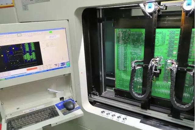
Bare board testing is a crucial quality control step in PCB manufacturing, where the integrity and functionality of the PCB's electrical connections are verified before the components are mounted. The process primarily involves two key tests: continuity testing and isolation testing.
Continuity Testing ensures that all electrical paths on the PCB are complete, meaning there are no open circuits that could obstruct current flow. Isolation Testing, on the other hand, checks for proper separation between different electrical connections to ensure there are no unintended shorts or leaks between them.
There are two common methods used for bare board testing in PCB manufacturing:
- Fixture Testing:
During fixture-based testing, a custom-built fixture with spring-loaded probes is used to simultaneously test all the electrical connections on the PCB. The fixture's top and bottom plates apply pressure to the probes, ensuring comprehensive coverage across the entire board. This method allows for testing thousands of points in parallel, making it highly efficient compared to other testing methods. Once the probes are set up, the test can be completed in as little as five seconds. This approach is ideal for high-volume production, offering both speed and accuracy. - Flying Probe Testing:
Flying probe testing uses robotic arms equipped with probes to verify the electrical connections on the PCB. The probes move across the board according to commands from specialized software, checking each connection. Flying probe testing is more flexible and cost-effective than fixture testing, making it ideal for smaller production runs or prototypes. While slower and more time-consuming than fixture testing, it is highly adaptable to different PCB designs and is particularly useful in cases where a more customized testing solution is needed.
Benefits of Bare Board Testing
Implementing bare board testing in the early stages of PCB design provides several key advantages, which can have a significant impact on both cost and production efficiency:
- Cost Savings:
By conducting thorough testing at the early design stage, manufacturers can identify potential issues before moving to assembly, helping to avoid costly rework or scrapping of defective PCBs. - Streamlined Production:
Early-stage issue detection allows designers and manufacturers to resolve problems during the prototyping phase, saving valuable time and resources in later stages of production. This proactive approach ensures smoother manufacturing and reduces delays caused by last-minute troubleshooting. - Enhanced Troubleshooting:
Bare board testing can pinpoint issues early in the design process, allowing engineers to trace problems back to their root causes with greater accuracy. This reduces the time spent on debugging and enables faster resolution of defects, leading to higher-quality end products.
In summary, bare board testing is an essential step for ensuring the electrical reliability of a PCB before it undergoes assembly, offering both cost and time efficiency benefits in the long run. Whether using fixture or flying probe testing, the process helps manufacturers maintain high quality standards and minimize production setbacks.
When to Consider Bare Board Testing for PCB?
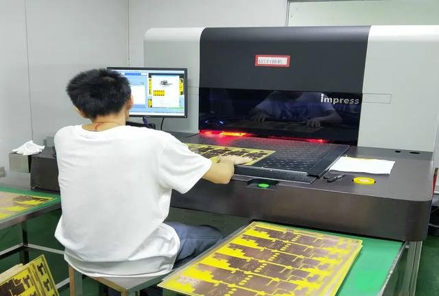
Integrating bare board testing early in the PCB development process can significantly enhance both the design and production workflows. It is particularly valuable during the initial design stages, as it allows for the early detection of potential issues, ultimately saving both time and costs. By incorporating bare board testing from the outset, manufacturers can streamline multiple aspects of the production process, resulting in higher efficiency and fewer delays later on.
Performing bare board testing during the early phases of PCB development enables designers to identify and rectify connectivity issues or design flaws before moving to the more complex and costly stages of assembly. This proactive approach reduces the risk of encountering larger, more expensive problems in the final stages, ensuring that the PCB is both functional and optimized for its intended purpose.
By adopting bare board testing at the right stage, companies can avoid unnecessary revisions, improve overall product quality, and achieve faster time-to-market, all while maintaining cost-effectiveness throughout the development cycle.
Why Choose CustomPCBA for Your PCB Services
When selecting a PCB supplier that aligns with your testing requirements, CustomPCBA stands out for its expertise in providing both prototype and small-batch production services. We are committed to delivering high-quality PCBs that meet your specific needs, whether it's for initial testing or scaling up to full production.
To learn more about our capabilities and how we can support your PCB development process, we invite you to request a quote online. Our team is ready to offer tailored solutions that ensure the efficiency and success of your project from design to production.

