Designing the layout of a printed circuit board (PCB) is crucial for creating a reliable and cost-effective circuit. While circuit design and component selection play important roles, allocating sufficient time for PCB layout is essential. Achieving the optimal layout requires careful consideration of several factors, particularly as modern circuit boards become increasingly complex, compact, and lightweight. The growing popularity of flexible PCBs has added an additional layer of complexity to this process.
Failing to account for critical layout considerations can result in a design that struggles to perform effectively in real-world applications. Improper PCB layout may lead to a range of issues, including electromagnetic interference (EMI), component conflicts on both sides of the board, limited functionality, or even complete board failure. Additionally, if the layout is not done correctly from the outset, redesigns will be necessary, potentially causing delays in manufacturing and increased costs.
So, what key PCB layout rules and considerations should you keep in mind? Let’s explore the essential steps involved in PCB layout design, highlighting the crucial points to consider at each stage. While other considerations may also be important, these are some of the most critical aspects of PCB layout design that you need to be aware of to ensure the success of your project.
Basic PCB Design Process
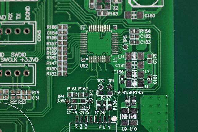
From the moment you determine the need for a PCB to its final production, PCB design plays a critical role in every step of the manufacturing process. The fundamental design process can be broken down into six key stages.
- Conceptualization
The first step is to define the overall concept of the PCB once its need has been established. This initial phase involves outlining the functions the PCB will perform, its features, how it will interface with other circuits, its placement within the final product, and its approximate size. Environmental considerations, such as the expected temperature range and potential external factors, should also be taken into account during this stage. PCB Layout Considerations: At this stage, the broad goals and requirements for the PCB’s design are established. - Schematic Design
In the schematic design phase, you create a circuit diagram that outlines all of the electrical components necessary for the PCB to function properly. This schematic includes detailed information on each component, such as their names, values, ratings, and part numbers from the manufacturer. During this phase, a Bill of Materials (BOM) is also compiled. The BOM contains all the required components for the PCB, and it’s essential to keep both the schematic and the BOM up to date as the design evolves. - Board-Level Diagram
The next step is to create a board-level diagram, which defines the physical dimensions of the PCB. This diagram includes labels for each section, marking areas designated for specific components. It also takes into account any electrical or space limitations. Grouping related components together helps ensure that routing is as short and efficient as possible. - Component Placement
Component placement determines the positioning of each electrical component on the PCB. It’s essential to consider factors such as signal flow, thermal management, and ease of manufacturing. Typically, several iterations of the component placement process are required to fine-tune the design and optimize space utilization. - Routing
The routing phase involves determining the paths for signal traces and setting routing priorities. Careful planning ensures the board’s signals are efficiently routed and that signal integrity is maintained. You will also need to address constraints such as minimizing trace lengths, avoiding interference, and optimizing power delivery. - Testing
Once the design is complete, a thorough round of testing is crucial to ensure the PCB meets all specified requirements. This testing phase may include electrical, thermal, and functional tests. If the design passes all tests, it can proceed to production. If issues arise, the design is revisited and adjusted until it satisfies all necessary criteria.
By following these steps, you ensure that your PCB design is optimized for functionality, manufacturability, and performance. Each stage plays a vital role in delivering a high-quality, reliable final product.
PCB Design Documentation
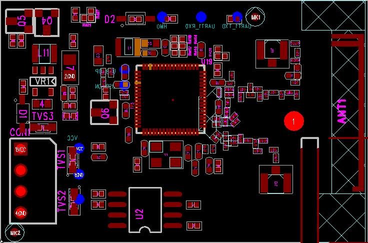
During the PCB design process, a substantial amount of documentation is developed to ensure that the design is well-documented, manufacturable, and functional. Below are the key documents typically generated:
- Hardware Dimension Drawing
This document outlines the physical dimensions of the bare PCB, including length, width, and any necessary cutouts or mounting holes. It serves as the blueprint for the PCB layout and provides manufacturers with the precise measurements required for fabrication. - Schematic Diagram
The schematic diagram represents the electrical characteristics of the PCB. It shows the connections between all components, including their values, ratings, and part numbers. This document is crucial for understanding the circuit’s design and for troubleshooting or modification during the development process. - Bill of Materials (BOM)
The BOM is a comprehensive list of all components required to assemble the PCB, including passive and active components, connectors, and any other materials necessary for the build. It includes details like part numbers, suppliers, quantities, and component specifications. An up-to-date BOM is critical for both procurement and assembly. - Layout Files
These files define the basic layout of the PCB, including the placement of components and routing of signal traces. They serve as the primary document for PCB manufacturers to follow during the fabrication process and help ensure the design is implemented correctly. - Component Placement Files
This document specifies the exact locations for each component on the PCB. Accurate component placement is critical for signal integrity, thermal management, and ease of assembly. It also helps with avoiding interference between components and optimizing the overall design. - Assembly Drawings and Instructions
Assembly drawings provide a visual guide for how the PCB should be assembled. They typically include component placement, soldering instructions, and any additional assembly considerations (e.g., component orientation, mounting instructions). These drawings are essential for PCB assemblers to understand the build process. - User Manual
Although not always required, a user manual can be extremely helpful for providing additional information on the operation, installation, and maintenance of the PCB. It can also include troubleshooting tips and usage guidelines, making it an important resource for end users. - Gerber File Set
Gerber files are a collection of output files that describe the physical layout of the PCB. These files provide the data necessary for PCB manufacturers to fabricate the board, including information on copper layers, silkscreen, solder mask, drill holes, and other critical features. Gerber files are the industry standard for PCB manufacturing.
Each of these documents plays a crucial role in the successful design, production, and eventual deployment of the PCB. Proper documentation helps streamline the design process, ensures the final product meets all requirements, and facilitates collaboration between designers, manufacturers, and users.
Best Practices for PCB Layout Design
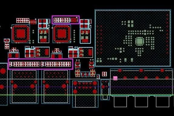
When designing a PCB, various factors must be taken into account to ensure optimal performance, manufacturability, and cost-effectiveness. These considerations span across different stages of the design process, and certain factors are specific to individual steps. Below are seven key factors to consider when creating a reliable and efficient PCB layout.
- Board Constraints
The first step is to define the physical constraints of the PCB. This includes determining the size and shape of the bare board. The available space, required functionality, and the product's form factor will dictate the board's dimensions. As electronic devices become smaller, it’s essential to estimate the board size early in the design process. If a simpler design doesn’t provide enough room for all necessary functions, a multi-layer or high-density interconnect (HDI) approach may be required. Although rectangular PCBs are the most common, custom shapes can also be designed to fit specific product requirements or space constraints. Be sure to factor in the number of layers your design needs early in the process, as more layers may be required for complex designs but will increase production costs. For high-current paths, ensure that at least two vias are used to facilitate layer transitions, which improves reliability, heat dissipation, and minimizes resistance and inductive losses. - Manufacturing Process
The choice of manufacturing process is another critical consideration. Different PCB fabrication techniques come with varying limitations and constraints. Ensure that the vias and holes used in the design are compatible with the chosen manufacturing process, and avoid placing components in vias to prevent interference. Additionally, the assembly method must be considered, as some techniques may require dedicated areas on the PCB to be kept free for placement or heat dissipation. If your design requires advanced techniques like multi-layer or flexible PCBs, it’s important to consult with your manufacturer to confirm that they have the necessary capabilities to produce the desired board type. - Materials and Components
The materials and components chosen for the PCB layout can significantly influence the design. Ensure that the required materials are readily available and that their cost is within budget. Some components may have specific design requirements, such as special footprints or spacing, so selecting the right parts that align with the PCB layout is essential. Take the time to choose the best materials for your specific application to ensure that your PCB design maximizes the performance of the selected components. - Component Placement Order
The order in which components are placed on the PCB is crucial for the layout's efficiency and overall performance. The general rule of thumb is to begin placing connectors, followed by power components, precision circuits, critical components, and then the remaining parts. Factors such as power levels, noise sensitivity, and signal integrity should be considered when prioritizing the placement sequence. - Orientation
For ease of assembly and to prevent errors during the soldering process, align similar components in the same direction. This practice will streamline the assembly process and reduce the risk of incorrect component orientation, which can lead to faulty circuits. - Component Positioning
Avoid placing components on the PCB solder side, especially when there are vias or through-hole components beneath them. Such placements can complicate assembly, reduce the reliability of the connections, and potentially block the necessary pathways for heat dissipation. - Organization and Layout
Effective organization of components on the PCB is vital for reducing the complexity of assembly, enhancing efficiency, and minimizing costs. Try to segregate surface-mount components (SMT) on one side of the board, while placing through-hole components on the opposite side. This practice simplifies the assembly process and improves the overall layout.
By paying careful attention to these PCB layout best practices, designers can avoid common pitfalls, reduce manufacturing delays, and ensure that the final product is both functional and cost-efficient. Thoughtful layout design also ensures that the PCB performs optimally across its intended lifespan, contributing to the overall success of the electronic product.
Considerations for Power, Ground, and Signal Routing in PCB Design
When designing a PCB, power, ground, and signal routing are fundamental aspects that significantly influence the board's overall performance and reliability. Proper routing ensures that signals are transmitted effectively, minimizing issues such as interference and signal degradation. Below are five crucial factors to consider when laying out these critical connections in your PCB design.
1. Power and Ground Planes
A key rule in PCB design is the proper placement of power and ground planes, typically within the internal layers of the board. These planes should be centrally located and symmetrically arranged to prevent warping, which can lead to component displacement and potential damage. For each power rail, ensure a common trace or bus bar is used for routing, and avoid chain-like (daisy-chain) connections between components. This will help maintain a low-impedance, stable power supply.
Separating power and ground planes, particularly for different voltage levels, is essential to prevent cross-interference. For example, keep high-power circuits isolated from low-power or sensitive signal circuits. If the ground plane is placed on a mid-layer, include a small-impedance path at the interface to prevent the coupling of noise from the power circuits. Additionally, keep analog and digital grounds separate as much as possible, allowing only signal traces to cross between them. This minimizes the risk of capacitive coupling, which could distort signals.
2. Track Routing
Signal tracks should be as short and straight as possible to maintain signal integrity and minimize loss. In cases where the board requires multiple signal paths, ensure that they cross at right angles rather than running parallel to one another. Parallel traces can induce unwanted coupling, which may result in crosstalk and signal degradation.
When calculating track widths, use specialized tools or calculators to ensure that traces can handle the necessary current levels without excessive heating or voltage drops. A 10 mil (0.010") trace might carry around 1 amp, while a 250 mil trace could handle up to 15 amps. Consider the thermal load and current demands when designing tracks, and ensure that high-current traces are sufficiently wide to prevent overheating.
3. Pad and Via Sizes
Early in the design process, determine the appropriate pad and via sizes for your components. The ratio of pad size to via hole size is crucial, especially for through-hole vias. As pad sizes shrink, the aspect ratio (the ratio of the via hole diameter to the pad size) becomes more critical. This ensures that the pads maintain reliable electrical connections and allow for proper soldering.
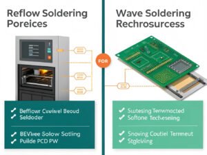
Consider the manufacturing process when choosing pad shapes. For instance, wave soldering typically requires larger pad areas compared to infrared reflow soldering, due to the difference in heat transfer characteristics. Ensure that your design adheres to the manufacturer’s specifications to avoid fabrication issues.
4. Signal Integrity and RF Considerations
Signal integrity is one of the most important aspects of high-speed PCB design, especially when dealing with high-frequency signals or RF circuits. The layout should minimize the potential for interference, noise, and crosstalk, all of which can significantly affect the performance of sensitive signals.
To avoid these issues, carefully plan the routing of high-frequency signals, avoiding parallel tracks that could couple and introduce noise. When signals must cross, ensure they do so at 90-degree angles to reduce parasitic capacitance and inductance. For critical signal paths, use ground planes or shielding to protect the traces from external interference.
In RF designs, minimizing large current loops and antennas is crucial. These large loops can radiate electromagnetic energy, which can affect signal quality and cause unwanted interference. Place components and traces carefully to minimize the loop area, and where possible, use dedicated ground planes for shielding. For multi-layer PCBs, a continuous ground plane is invaluable for maintaining signal integrity.
5. Thermal Management
Thermal considerations are critical for ensuring the long-term reliability of your PCB. Higher power densities and more complex designs often lead to greater heat generation, which can cause components to overheat and malfunction if not properly managed.
To manage heat dissipation, identify components that generate significant heat early in the design process. Refer to component datasheets to understand their thermal characteristics, such as thermal resistance, and ensure the layout accommodates heat management strategies. For high-heat components, allow ample space around them to facilitate airflow and heat dissipation.
To improve thermal performance, use thermal vias to channel heat from high-power components to the bottom layers or copper pours. These vias should be placed close to heat-generating components. If necessary, add heat sinks, thermal pads, or fans to assist with cooling. For multi-layer designs, copper pours on the internal layers can help spread heat more evenly across the board.
In summary, effective power, ground, and signal routing are vital to the success of a PCB design. By considering these aspects during the design phase, you can ensure that the PCB will operate reliably, with minimal interference, signal degradation, or thermal issues. Proper planning and attention to detail in these areas contribute to a more robust and efficient final product.
Using CAD to Optimize PCB Layout Design
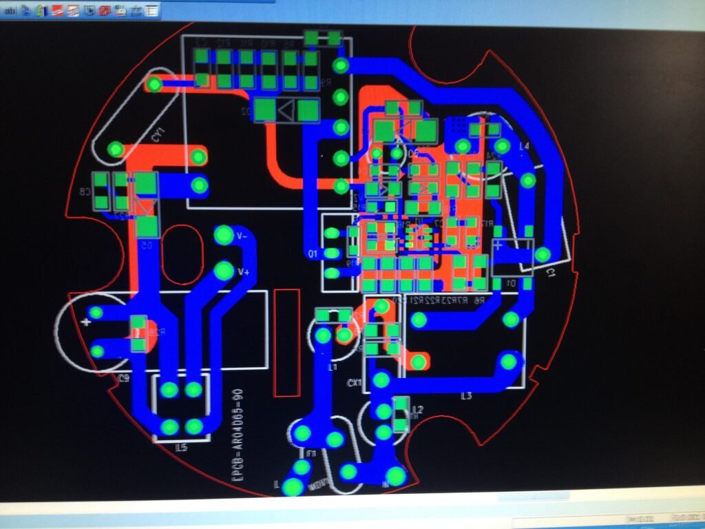
Most modern PCB designs rely on CAD software, offering several advantages in both design and manufacturing:
- Streamlined Design Process: CAD software allows for drag-and-drop component placement and automatic routing, speeding up design and reducing human errors.
- Design Verification: CAD tools help detect design errors (e.g., component spacing, trace rules) before production, ensuring the design meets requirements.
- Manufacturing File Generation: CAD software can automatically generate necessary manufacturing files (like Gerber files), improving accuracy and easing the transition to production.
- Documentation and Version Control: CAD systems track design changes and version control, facilitating future maintenance and collaboration.
- Rule and Template Creation: Designers can create custom rules and templates to improve design consistency and efficiency.
Choosing a PCB Supplier
By using CAD software, designers can boost efficiency, lower production costs, and ensure the quality and accuracy of their designs.
If you're in need of high-quality printed circuit boards (PCBs), CustomPCBA is your ideal partner. We offer a comprehensive range of PCB capabilities tailored to meet the specific needs of your project, and we're committed to delivering exceptional customer service. With both domestic and international PCB manufacturing options, we provide flexible financing solutions and quick turnaround times. Whatever your choice, you can trust that you'll receive only the highest quality PCB products.
To learn more about our PCB services and how we can support your business, please provide detailed project information (including Gerber files) for a quote. We also offer free design checks via our website to ensure your design is ready for manufacturing. For more information about CustomPCBA and our wide array of services, feel free to contact us for a quote or continue exploring our website.

