
Circuit Board Testing in PCBA Manufacturing
Circuit board testing plays a crucial role in the printed circuit board assembly (PCBA) manufacturing process. By conducting systematic testing before products are delivered to end users, manufacturers can identify and rectify potential issues, ensuring product integrity and customer satisfaction. As electronic products become increasingly complex and multifunctional, selecting the right circuit board testing methods becomes essential. This article explores some common testing methods, their advantages and disadvantages, and suitable applications.
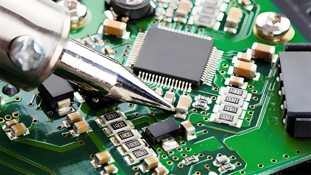
1. Visual Inspection
Visual inspection is the initial step in circuit board testing. It involves examining the PCBA using the naked eye, magnifying tools, or automated optical inspection (AOI) systems.
Advantages:
- Quick and Efficient: Visual inspection can be performed rapidly, making it suitable for fast-paced mass production.
- Cost-Effective: Compared to other testing methods, visual inspection requires relatively low investment.
- Wide Applicability: It can identify a variety of obvious defects, including misaligned components, solder bridging, and missing or damaged parts.
Disadvantages:
- Limited Detection Capability: Visual inspection may miss faults that are difficult to see with the naked eye, especially those hidden beneath components.
- Subjectivity: Results may vary based on individual experience and eyesight, leading to inconsistency.
Suitable Applications: Visual inspection is ideal for preliminary screening and identifying apparent defects, especially in large-scale production where it can quickly eliminate most significant issues.
2. Functional Testing
Functional testing involves applying voltage and signals to the circuit board to verify whether it operates according to its intended functions.
Advantages:
- Comprehensive Assessment: Functional testing can validate the actual functionality of the circuit board, ensuring all components work correctly.
- High Accuracy: By simulating real operating conditions, it can accurately detect potential issues.
Disadvantages:
- Higher Cost: Setting up testing equipment and developing test programs requires time and financial investment.
- Longer Testing Duration: Compared to visual inspection, functional testing typically takes more time.
Suitable Applications: This method is suitable for high-end electronic products that require assurance of faultless operation, particularly in industries such as aerospace, medical, and automotive.
3. Short and Open Circuit Testing
Short and open circuit testing focuses on verifying the connectivity of the circuit board to ensure the integrity of various circuit paths.
Advantages:
- Simple and Effective: This method can quickly detect short circuits and open circuits in the circuit.
- High Reliability: The test results directly reflect the connectivity of the circuit, offering high accuracy.
Disadvantages:
- Limited Issue Detection: This testing method cannot identify functional deficiencies of components or other types of faults.
Suitable Applications: It is applicable in the early stages of circuit board production to ensure that the basic electrical connections are intact.
4. Programming Testing
For circuit boards requiring firmware or software, programming testing is an essential step. This test involves burning a program onto the circuit board to check if its software functions correctly.
Advantages:
- Comprehensive Functionality: It tests not only hardware but also software performance.
- User Experience Validation: By testing user scenarios, it ensures product stability in real-world use.
Disadvantages:
- Time and Resource Intensive: The programming and testing processes require significant time and resources.
- High Complexity: It necessitates skilled personnel to conduct the tests, increasing labor costs.
Suitable Applications: This method is suitable for complex electronic products that require firmware or software support, such as smart devices and embedded systems.
High-quality electronic products depend on effective testing methods. Visual inspection, functional testing, short and open circuit testing, and programming testing each have their advantages, disadvantages, and specific applications. Manufacturers must assess their project needs and combine the strengths of different testing methods to develop suitable circuit board testing strategies. This not only helps improve the efficiency of the PCBA manufacturing process but also significantly enhances the overall quality of the final product and customer satisfaction. In today’s competitive market, ensuring the reliability and performance of electronic products is key to gaining customer trust and market share.
Identifying Faults in Completed Assembled PCBs
Assembled PCBs (Printed Circuit Boards) refer to circuit boards where all electronic components have been installed and soldered. These components are interconnected to form an electrical system, enabling the PCB to perform specific functions. However, faults in the circuit board can significantly impact the overall performance of the assembled PCB, making it essential to understand and identify these faults. Below are three common categories of faults along with their in-depth analysis.
1. Component Failures
Component failures refer to individual electronic components that fail to function properly, which can be caused by various factors:
- Poor Material Quality: The use of low-quality components can lead to unstable performance or failure. For example, inferior resistors may cause current overloads, while substandard capacitors may fail to filter signals effectively.
- Manufacturing Errors: If components are improperly installed during production (e.g., incorrect soldering positions or polarity errors), they may not operate as intended. These errors are often due to human mistakes or faults in automated equipment.
- Damage During Transportation and Assembly: External shocks or vibrations during transportation can damage components, resulting in decreased performance or complete failure.
To effectively identify component failures, advanced testing equipment such as Automatic Optical Inspection (AOI) systems and X-ray inspection can be used to ensure the integrity of each component.
2. Manufacturing Defects
Manufacturing defects typically arise from non-compliant production processes, with common types including:
- Poor Solder Joints: Using inappropriate solder or improper soldering techniques can lead to weak or cold solder joints, affecting the reliability of electrical connections.
- Misalignment of Components: If components are not aligned correctly during placement, it can result in short circuits or open circuits. This is particularly critical in high-density PCBs, where precise alignment is essential.
- Insufficient Solder Paste Application: Uneven application of solder paste on the PCB can cause some components to connect poorly, impacting overall performance.
Manufacturing defects can be minimized through stringent quality control measures and the use of modern testing technologies, such as Solder Paste Inspection (SPI) and In-Circuit Testing (ICT).
3. Performance Failures
Although a circuit board may appear to function normally, performance failures can occur due to design or environmental factors:
- Circuit Design Errors: Mistakes made during the design phase can prevent the circuit from operating correctly under expected conditions. This includes inappropriate component selection or inefficient circuit layout.
- Poor Thermal Management: If the PCB design does not effectively dissipate heat, certain components may overheat, shortening their lifespan. Proper thermal design and thermal simulation analysis can help address this issue.
- Electromagnetic Interference (EMI): External electromagnetic interference can negatively impact the performance of the PCB, especially in high-frequency applications. Using shielding and appropriate grounding techniques can mitigate these problems.
When facing performance failures, system-level testing and simulation tools can provide valuable insights to help identify potential issues.
While careful manufacturing processes and quality control can significantly reduce faults, adopting advanced PCB testing methods is essential in modern electronic products. These methods not only facilitate the rapid identification of faults but also ensure product quality before market release. By thoroughly understanding the different types of faults, manufacturers can implement more effective detection and repair strategies, ultimately enhancing product performance and customer satisfaction.
Enhancing Early Fault Detection in PCB Assembly
As competition in the electronics industry intensifies, early fault identification becomes crucial for optimizing resource allocation and maximizing return on investment. The ability to promptly discover and correct defects can save significant time, effort, and money, providing companies with a strategic advantage. One effective approach to facilitate efficient testing of Printed Circuit Board Assemblies (PCBA) is the concept of Design for Testability (DFT).
DFT is a proactive design strategy that incorporates testing and troubleshooting considerations during the design of electronic circuits and components. This approach simplifies the identification and rectification of potential issues while increasing overall test coverage and reducing time-to-market, ultimately enhancing product quality. Key elements of DFT include:
1. Accessibility of Test Points
Ensuring that test points—specific locations on the PCBA for connecting testing equipment—are easily accessible is vital to DFT. Proper placement of test points enables efficient testing while minimizing interference from adjacent components. Engineers should pay particular attention to the distance between taller components and test points to prevent signal disruption during testing.
2. Integration of Testability Features
Incorporating testability features such as Built-In Self-Test (BIST) circuits significantly enhances fault detection and diagnosis efficiency. These functionalities allow devices to perform self-checks without relying on external testing equipment, which is especially important in critical systems. Moreover, BIST features provide real-time feedback, aiding engineers in identifying potential issues at an early stage, thereby reducing later maintenance costs.
3. Simplifying the Design Process
Reducing the complexity of circuits and components is an effective strategy for simplifying PCBA design. By employing modular designs and minimizing the number of unique components, engineers can enhance design flexibility while making testing and troubleshooting more manageable. Additionally, simplifying designs helps mitigate production errors, improving overall manufacturing efficiency.
4. Hierarchical Design
Organizing PCB designs into functional blocks or modular structures improves testability. By breaking the design down into smaller, independent sections, engineers can more easily locate and address sources of faults. Modular design also allows companies to reuse these functional blocks in future projects, speeding up the design process and reducing the risks associated with new product development.
5. Adequate Spacing and Layout
Maintaining proper spacing between components and optimizing their layout is critical for enhancing testing effectiveness. Appropriate spacing can reduce the risks of signal interference and heat buildup, thereby decreasing the likelihood of failures due to components being too close together. Furthermore, optimized layouts can improve assembly efficiency and reduce complexity in the manufacturing process.
6. Employing Advanced Testing Technologies
To further enhance fault detection accuracy, adopting advanced testing technologies and equipment is essential. For example, using Automated Optical Inspection (AOI), X-ray inspection, and In-Circuit Testing (ICT) can efficiently identify potential issues and provide detailed fault analysis. These technologies not only improve testing comprehensiveness but also significantly shorten detection times.
By thoroughly exploring the importance of identifying faults in loaded PCB components and the value of integrating Design for Testability principles, companies can adopt more comprehensive and efficient testing strategies. This not only aids in enhancing the efficiency of fault identification but also ensures that products possess exceptional quality before entering the market, ultimately providing companies with greater competitive advantage.
Common Circuit Board Testing Methods
Here’s a summary table of common PCB testing methods that compares the advantages and disadvantages of each method, as well as their most suitable application scenarios.
| Testing Method | Advantages | Disadvantages | Best Use Cases |
|---|---|---|---|
| Visual Inspection |
– Fast and cost-effective – Can identify various defects (e.g., misaligned components, solder bridges) |
– May overlook faults not visible to the naked eye – Difficult to inspect complex PCBs |
– Preliminary screening in mass production – Identification of severe defects |
| Automated Optical Inspection (AOI) |
– Efficient and quick, can automate defect identification – Capable of comprehensive inspection |
– Limited ability to detect fine defects – High initial investment cost |
– Small to medium batch production – Products requiring high precision |
| X-Ray Inspection |
– Can deeply inspect internal solder joints and components – Helps identify hidden defects |
– Expensive equipment, complex operation – Requires high operator skill level |
– Multi-layer PCBs or complex packaging – Products with very high quality requirements |
| In-Circuit Testing (ICT) |
– Provides comprehensive testing of PCB functionality – Offers detailed fault analysis |
– High requirements for test points – Significant initial investment and preparation work |
– Functional testing of complex PCBs – Quality control in mass production |
| Functional Testing |
– Validates product performance under real operating conditions – Provides real-use feedback |
– Longer testing time, higher cost – Cannot detect all electrical defects |
– Verification testing during product development – Final inspection of products |
| Environmental Testing |
– Assesses PCB reliability under extreme conditions – Detects environmental impacts |
– Requires complex testing equipment – Longer testing time |
– Products with high reliability requirements – Aerospace or military applications |
| Thermal Imaging Inspection |
– Can monitor component temperatures in real-time – Helps discover overheating issues and design flaws |
– Cannot replace other testing methods – Provides only surface information |
– Fault-finding phase – Thermal management evaluation of electronic products |
Common PCB Testing Methods: A Comparative Analysis

In-Circuit Testing (ICT)
In-Circuit Testing (ICT) is an advanced testing method that employs a specialized fixture known as a “bed of nails” to establish electrical connections with designated test points on the Printed Circuit Board Assembly (PCBA). This fixture ensures accuracy and consistency in testing by making direct contact with the test points.
ICT devices can evaluate various electrical characteristics, including resistance, capacitance, and inductance, effectively identifying faults such as short circuits, open circuits, or incorrect component values. Its primary advantage lies in providing a high level of test coverage and precision, making it highly valued in demanding manufacturing environments. However, the need to design and develop custom test fixtures for each specific PCBA can be time-consuming and resource-intensive, leading to increased initial investment costs. Thus, while ICT excels in performance, its high upfront costs may limit its use by some small to medium-sized enterprises.
Flying Probe Testing (FPT)
Flying Probe Testing (FPT) is a flexible, non-contact testing method that uses a set of movable probes to make electrical contact with test points on the PCBA. These probes move across the circuit board, systematically checking each test point in a predefined sequence, enabling a quick and efficient testing process.
The main advantage of FPT is that it does not require custom fixtures, making it particularly suitable for small to medium batch production or prototype development. This method not only reduces production costs but also enhances flexibility, allowing engineers to quickly adjust testing plans to accommodate different PCB designs. However, a notable drawback of FPT is its relatively slower testing speed, which may not provide the same level of test coverage and accuracy as ICT. Therefore, in highly demanding production environments, FPT may not be the best option.
Summary
Whether using In-Circuit Testing or Flying Probe Testing, selecting the appropriate testing method should take into account production scale, budget constraints, and product complexity. ICT offers higher accuracy and coverage but comes with high costs and time investments that may not suit all applications. On the other hand, FPT excels in flexibility and cost-effectiveness, making it ideal for rapid prototyping and small-batch production. By understanding the characteristics of each method, manufacturers can make informed choices based on their needs, ensuring the quality and reliability of the final product.
How to Choose the Right Testing Solution
Selecting the appropriate testing method for your Printed Circuit Board Assembly (PCBA) is crucial to ensuring that your electronic products function as intended. While your Contract Manufacturer (CM) can assist you in this decision, it’s essential to consider the following factors to make an informed choice:
1. Project Requirements
Understanding the specific requirements of your project is paramount. This includes the desired level of testing accuracy, coverage, and any unique factors related to the PCBA design. Consider the complexity of the circuit, the types of components used, and the intended application of the PCBA. For instance, if your product demands high reliability in a critical application, more rigorous testing methods may be necessary.
2. Production Volume
The volume of production significantly influences which testing method will be most effective. For high-volume manufacturing, In-Circuit Testing (ICT) often proves to be the better option due to its accuracy and extensive coverage of test points. Conversely, for low-volume runs or prototyping, Flying Probe Testing (FPT) offers the flexibility needed without the necessity for expensive custom fixtures. Assessing your production scale will help you determine the most efficient and cost-effective approach.
3. Budget Considerations
Cost is a critical factor when choosing a testing method. While some methods may offer higher accuracy and broader coverage, they often come with the price of expensive custom equipment. It’s important to evaluate the total cost of each method, including both initial setup costs and ongoing operational expenses. A thorough cost-benefit analysis can help identify the best value for your specific needs.
4. Test Accessibility
Examine the layout and design of your PCBA to identify any potential limitations that could impact your choice of testing method. For example, Boundary Scan (JTAG) is particularly effective for accessing high-density digital PCBs where physical access to test points is limited. Other testing methods might be more suitable for designs that allow for easier access to test points. Ensuring that your chosen method aligns with the physical constraints of your design can enhance testing efficiency.
5. Turnaround Time
Consider the timeline you have available for the project. Some testing methods may require longer setup and execution times. For instance, ICT typically necessitates the creation of custom fixtures, which can lead to longer lead times. In contrast, FPT is renowned for its quick setup, allowing for faster testing cycles. Evaluating your timeline and urgency will help determine which method can meet your deadlines effectively.
By carefully considering these factors—project requirements, production volume, budget, test accessibility, and turnaround time—you can make a well-informed decision about the most suitable testing method for your PCBA. This strategic approach will not only enhance the quality and reliability of your electronic products but also align with your overall production goals and customer satisfaction.
Achieving Efficient and Cost-Effective Testing Strategies
In PCB testing, it is crucial to ensure the optimal balance between test coverage and cost. Comprehensive testing typically leads to higher reliability and fewer defects; however, it also increases the overall project costs, which may include the need for custom test fixtures, specialized testing equipment, and extended testing cycles. Therefore, finding an efficient and economical testing solution is the goal of every electronic product developer.
Here are some effective strategies to help achieve high testing coverage without exceeding the budget:
- Identify Key Testing Areas:
- For each PCBA design, identifying the most critical testing areas is a primary task. Focus on components and functions that could impact product performance, ensuring that these critical areas achieve the highest level of testing coverage. Conducting risk assessments helps identify high-risk zones, allowing you to allocate more resources for testing, thereby reducing potential failures.
- Utilize Multi-Layered Testing Methods:
- Combining various testing methods can effectively enhance testing coverage. For instance, initial production stages may involve visual inspections and functional testing, while more complex methods such as In-Circuit Testing (ICT) and Flying Probe Testing (FPT) can be introduced later. This phased testing strategy not only reduces costs but also adapts to different needs at various production stages, ensuring that every aspect is thoroughly validated.
- Implement Design for Testability (DFT):
- Considering testability during the design phase can significantly simplify subsequent testing processes. By optimizing circuit design to ensure the accessibility of test points, reducing interference between components, and improving testing convenience and effectiveness, this design strategy can save considerable time and costs in later testing stages.
- Conduct Dynamic Cost-Benefit Assessments:
- Continuously monitoring and evaluating the cost-effectiveness of selected testing methods is essential. By considering production volumes, budget constraints, and specific project requirements, regularly review the effectiveness of testing processes and equipment, and make timely adjustments to optimize resource allocation. Regular communication with the team to gather feedback ensures continuous improvement in the testing process.
- Prevent Hidden Costs:
- Neglecting certain aspects during testing may lead to long-term hidden costs, including product recalls due to missed defects, customer complaints, and increased after-sales service costs. These factors can adversely affect the company’s financial status and potentially damage its brand reputation. Therefore, implementing stringent testing standards and processes can effectively mitigate these potential costs.
By integrating these strategies, companies can enhance the overall quality and reliability of their products while controlling costs, ultimately achieving a higher level of market competitiveness. Ensuring that products undergo rigorous testing before market entry will provide long-term strategic advantages for the business.
Conclusion
To ensure the quality, reliability, and performance of electronic products, it is crucial to have effective PCB testing methods. In our discussion, we detailed several common testing approaches, including visual inspection, In-Circuit Testing (ICT), Flying Probe Testing (FPT), Functional Circuit Testing (FCT), and Boundary Scan (JTAG). Each method has its unique advantages and applicable scenarios, and the right selection and combination can significantly enhance testing effectiveness.
However, relying solely on these testing methods is not sufficient to comprehensively ensure product quality. Considering testing requirements during the design phase can help you effectively balance testing coverage, costs, and project demands. By incorporating Design for Testability (DFT) principles, you can not only improve the effectiveness of testing but also reduce the complexity and costs associated with the subsequent testing processes.
Furthermore, continuously monitoring the effectiveness and cost-efficiency of testing procedures is essential. Regularly assessing and adjusting testing strategies can ensure that your products consistently meet high-quality standards while satisfying customer expectations.
In summary, by integrating multiple testing methods and considering testability early in the design phase, you will be able to continuously produce high-quality electronic products that meet market demands. This proactive approach will not only enhance customer satisfaction but also strengthen your company’s competitive edge in a challenging market.
