Automated Optical Inspection (AOI) is an indispensable technology in modern electronics manufacturing, primarily used for quality control and defect detection in printed circuit boards (PCBs). AOI employs high-precision optical imaging systems, using multiple angles of illumination and photography to quickly and efficiently identify defects on PCBs, ensuring products meet quality standards before delivery. Below is a detailed analysis of AOI, including its working principle, advantages, applications, and comparisons with other inspection methods.
What is Automated Optical Inspection (AOI)?
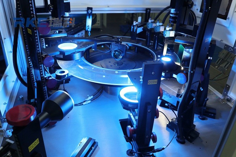
Automated Optical Inspection (AOI) is a technology that uses optical imaging systems to perform non-contact inspection of circuit boards. AOI systems shine light onto the PCB and capture the reflected light to generate images, which are then analyzed to detect defects. The technology automatically compares the PCB’s actual features with the ideal design (often based on CAD drawings), identifying potential manufacturing issues such as missing components, soldering defects, misaligned parts, etc.
How AOI Works
AOI systems typically consist of multiple light sources and cameras. Light sources illuminate the PCB from various angles, ensuring comprehensive capture of surface and internal details. Static or dynamic images are captured, processed in real-time, and compared to reference images to detect discrepancies.
In practical applications, AOI scanning is fully automated, which significantly enhances inspection speed and accuracy. Compared to traditional manual visual inspections, AOI can detect even the smallest defects and perform comprehensive scans without damaging the PCB. This makes AOI a vital inspection tool in the PCB manufacturing process.
AOI Application Stages
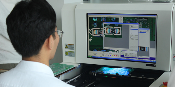
AOI plays a key role throughout the PCB manufacturing process, particularly in the following stages:
- Bare Board Inspection: AOI can detect defects in the PCB’s pads and layout before it is assembled, ensuring a smooth production flow.
- Solder Paste Inspection: AOI can detect whether the solder paste is applied evenly and whether there is too much or too little paste, preventing soldering issues in later stages.
- Pre-Reflow Inspection: Before the PCB enters the reflow soldering stage, AOI can check if components are placed correctly, avoiding errors during reflow.
- Post-Reflow Inspection: After reflow soldering, AOI can inspect solder joints for defects such as solder bridges, poor joints, or cold soldering.
AOI Inspection Content
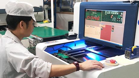
The main function of AOI is to identify all defects that deviate from the PCB design. Some of the common defects detected by AOI include:
Soldering Defects
- Open Circuits: When there is a break in the circuit, preventing current flow. AOI can precisely detect any part of the circuit that is not connected properly.
- Solder Bridges: When solder accidentally connects two pads that should remain separate, leading to a short circuit or other electrical issues. AOI can detect even small solder bridges, preventing short circuits.
- Insufficient Solder: Inadequate solder can lead to unstable connections. AOI detects soldering issues by comparing the actual solder amount with the expected design, identifying solder shortages.
- Excessive Solder: Too much solder can cause solder bridges or other problems. AOI can accurately assess if excess solder is present and highlight areas for rework.
Component Defects
- Missing Components: If a component is missing from the PCB, AOI automatically flags it, ensuring that no PCB is sent out without its required components.
- Misalignment: AOI can detect if a component is improperly placed or shifted during assembly, ensuring the components are positioned correctly on the PCB.
- Lead Lifting: If a component lead does not make full contact with the solder, it may result in an unstable connection. AOI can detect lifted leads and flag them for rework.
Advantages of AOI
- High Precision and Efficiency: AOI can detect even the smallest defects without compromising production speed. It outperforms manual inspection in terms of speed and precision.
- Reduced Human Error: The human eye is limited in detecting small defects, especially in high-volume production. AOI reduces errors and omissions that might occur during manual inspections.
- Increased Production Efficiency: AOI’s automation significantly speeds up the PCB inspection process, reducing downtime and rework rates.
- Customizable Settings: AOI systems can be tailored to meet specific design requirements, ensuring they can detect particular types of defects according to the needs of each production line.
AOI Compared with Other Inspection Methods
When compared to other common inspection methods, AOI has several distinct advantages:
- Automated X-Ray Inspection (AXI): AXI uses X-rays to penetrate multi-layer PCBs, making it suitable for complex boards. However, AXI is more expensive and is typically used only for high-complexity PCBs. AOI is more cost-effective and suitable for most standard PCB inspections.
- Automated Laser Testing (ALT): ALT uses lasers to scan the PCB and assess solder paste distribution and volume. However, laser measurements can be influenced by environmental factors, which may lead to measurement errors. AOI, on the other hand, is more stable in handling complex shapes and surface reflections.
- In-Circuit Testing (ICT): ICT uses electrical probes to check the electrical connections on the PCB, directly verifying the functionality of the circuit. However, it cannot detect external physical defects such as excessive or insufficient solder. AOI offers a more comprehensive inspection by detecting both electrical and physical issues.
- Manual Visual Inspection (MVI): While manual inspection can detect obvious defects, it is slow and prone to error, especially in large-scale production. AOI’s automated nature ensures more accurate and efficient inspections, reducing the likelihood of human fatigue or oversight.
Conclusion
Automated Optical Inspection (AOI) plays a critical role in PCB production, offering high efficiency, precision, and automation. It not only detects soldering defects and component issues but also provides real-time feedback on potential problems during manufacturing, helping manufacturers adjust their processes accordingly. As electronic products become increasingly complex, AOI will continue to be a vital tool in the PCB production process, ensuring high-quality, reliable end products.

