
Pads are one of the smallest features on a PCB, yet they decide whether your components solder well and whether your board survives real-world use. I learned this many times while helping clients troubleshoot solder defects caused by pad size, spacing, or plating choices.
A pad is the exposed copper area on a PCB used to solder component pins or leads, enabling mechanical support and electrical connection.
Pads look simple, but choosing the right pad type, size, and finish is essential for stable manufacturing. Understanding them early saves you from solder issues, rework, and costly redesigns later.
What exactly is a pad in PCB design?
I often see beginners confuse pads with vias or copper pours. When the design enters manufacturing, this leads to shorts, poor solder joints, or tombstoning.
A PCB pad is a defined copper area where components are soldered. Pads link parts to traces, provide electrical contact, and secure components during assembly.
How pads work and why they matter in real production
Pads form the physical landing points for components. Every resistor, IC, connector, or sensor relies on well-designed pads.
A typical pad structure includes:
| Layer | Function |
|---|---|
| Copper | Creates electrical contact |
| Solder mask opening | Exposes copper for soldering |
| Surface finish (ENIG, HASL, etc.) | Ensures good solder wetting |
| Paste layer (SMT only) | Controls solder volume |
Pads influence:
- Solder joint strength
- Heat balance during reflow
- Component alignment
- Electrical reliability
- Long-term durability under stress
When customers send me files, pad issues are one of the most common DFM findings. Incorrect land patterns often cause defects like bridging, cold joints, or lifted pads. That’s why my engineering team always checks footprints, solder mask clearance, and paste apertures before production.
What are the different types of pads in PCB development?
Pads come in several forms depending on the component. Early in my career, I didn’t realize how these differences affect soldering. One project failed because the wrong pad type was used for a through-hole connector.
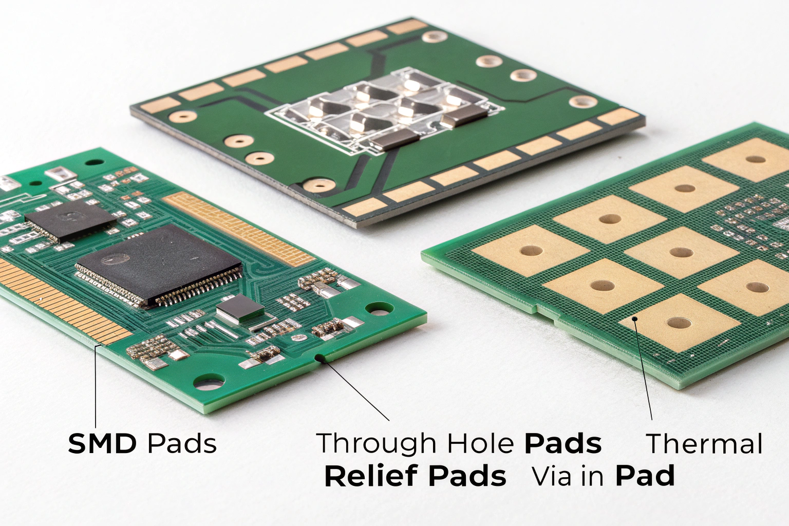
PCB pad types include SMD pads, through-hole pads, thermal relief pads, and via-in-pad structures, each designed for specific components and soldering methods.
A deeper look at pad types and when to use them
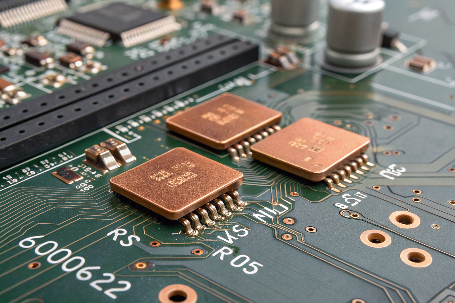
1. SMD Pads (Surface Mount Pads)
Copper pads for SMT components like resistors, ICs, and MOSFETs.
- Used in reflow soldering
- Pad size must match component land pattern
- Paste layer controls solder volume
2. Through-Hole Pads
Pads with drilled holes for components such as connectors or large capacitors.
- Strong mechanical support
- Used in wave or selective soldering
- Requires proper annular ring design
3. Thermal Relief Pads
Special pads connected to copper planes with narrow “spokes.”
- Prevents heat imbalance
- Reduces soldering difficulty
- Common in ground or power planes
4. Via-in-Pad
Vias placed directly inside pads, often filled and plated.
- Used for high-density designs, RF, or thermal dissipation
- Requires special filling to avoid solder wicking
- Common in small BGA packages
Summary table:
| Pad Type | Best Use Case | Notes |
|---|---|---|
| SMD pad | SMT parts | Controls solder amount |
| Through-hole pad | Connectors, large parts | Strong mechanical hold |
| Thermal pad | Power chips | Helps heat dissipation |
| Via-in-pad | BGA, RF | Requires filled vias |
Whenever customers ask for designs with BGAs or high-density chips, we carefully review via-in-pad to ensure the process meets stability requirements. This prevents solder loss during reflow and avoids hidden defects.
How do pad design choices affect soldering and reliability?
A pad may look like simple copper, but a small design mistake can cause major production failures. I have seen boards with perfect schematics fail simply because a pad was 0.1 mm too small.
Pad design affects solder joint quality, heat balance, component alignment, manufacturability, and long-term durability of the PCB.
How pad engineering influences real-world performance
1. Solder Volume
Pad size and paste aperture decide the amount of solder. Too much causes bridging; too little causes weak joints.
2. Heat Balance
Uneven pad sizes make components tombstone during reflow.
This happens often with 0402 or 0201 resistors.
3. Mechanical Strength
Large connectors or power components need reinforced pads and proper plating.
Without this, pads may peel off under stress.
4. Electrical Stability
Poor pad spacing risks shorts and noise issues, especially near high-speed ICs.
5. Surface Finish
ENIG gives better reliability for fine-pitch pads.
HASL is cheaper but may cause uneven plating for tiny pads.
In my factory, we always perform a footprint and pad review before manufacturing. We check:
- Annular ring size
- Solder mask opening
- Pad-to-pad spacing
- Via distance
- Solder paste design
- Expected thermal behavior during reflow
Customers often thank us because this early correction prevents expensive rework.
Conclusion
Pads may look small, but they control solder quality, electrical connection, and long-term durability. By choosing the right pad type, size, and finish, your board becomes easier to assemble and more reliable in daily use. With careful design and engineering support, you can avoid common defects and build stronger, more stable electronics that last.
