
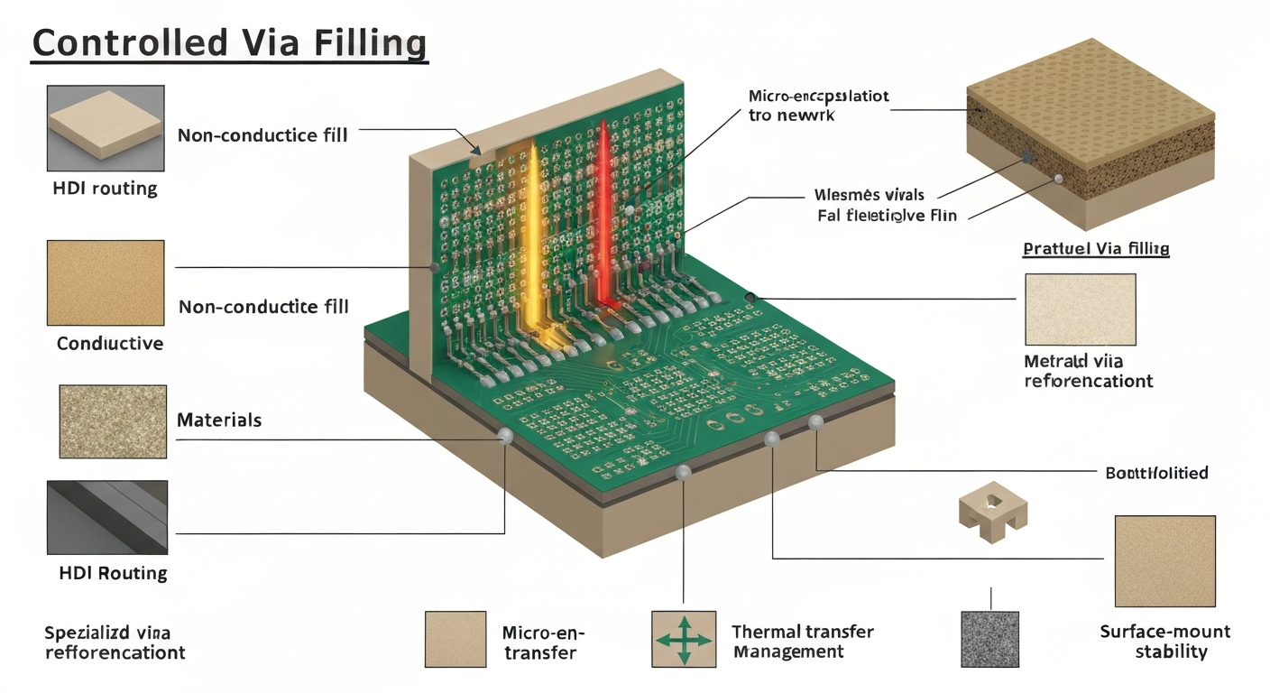
PCB via filling techniques control how vias are reinforced, insulated, or prepared for special functions such as HDI routing, thermal transfer, or surface-mount stability. These methods improve reliability, enable compact layouts, and support advanced assembly requirements.
Reliable via filling supports signal integrity, prevents solder leakage, and strengthens the board structure. When selected correctly, it helps meet performance, density, and manufacturability targets across prototypes and mass-production runs.
Why do PCB via filling techniques matter?
Vias become structural and electrical weak points if left untreated. Poor via management causes solder wicking, pad collapse, or long-term failure.
Via filling techniques matter because they protect the via barrel, improve assembly stability, and enable high-density layouts without risking defects.
Deeper Insight
Via filling determines how vias behave during soldering and operation. Standard open vias may trap flux, leak solder, or compromise pad strength during reflow. Filled vias solve these issues by reinforcing the via structure and sealing the hole.
Manufacturers use specific filling materials—conductive pastes, non-conductive resins, electroplated copper—to support HDI routing, prevent BGA collapse, or handle high thermal loads. Different industries require different approaches. Industrial control boards prioritize reliability, while IoT modules may prioritize compact routing or RF performance.
Factories with strong engineering support evaluate stack-ups, copper thickness, drill size, and assembly conditions to recommend the appropriate via filling method. This reduces redesigns, shortens prototype cycles, and stabilizes yield for both small-batch and mass-production customers.
What is non-conductive via filling?
Non-conductive filling is one of the most commonly used techniques for HDI and BGA designs.
Non-conductive filling uses epoxy resin to fill vias, providing mechanical stability while preventing solder wicking and improving pad surface quality.
Deeper Insight
Non-conductive resin fills the via barrel and cures to create a stable, insulated structure. This method keeps solder from flowing into the via during assembly, which helps maintain consistent pad height for BGA packages. It also strengthens the pad against mechanical stress and improves reliability under thermal cycling.
Designers use this filling technique for:
- BGA pads with via-in-pad
- High-density layouts with microvias
- Boards requiring clean SMT surfaces
- Applications where electrical conduction is not needed inside the via
Factories rely on resin filling because it supports reflow stability and allows smooth planarization for pad plating. CAM teams evaluate via aspect ratios, resin expansion rate, and copper balance to avoid voids or delamination.
For B2B buyers building compact IoT modules, sensor boards, or communication devices, non-conductive filling ensures stable BGA solder joints and reduces long-term field failures.
What is conductive via filling?
Conductive via filling improves electrical and thermal performance but requires strict process control.
Conductive via filling uses silver-based or copper-enhanced epoxy to create a conductive path that supports heat transfer and current flow.
Deeper Insight
Conductive filling is preferred for applications requiring heat dissipation or stronger electrical performance inside the via. Silver epoxy is commonly used due to its high conductivity. After filling, the surface is planarized and sealed for soldering.
This method supports:
- Power circuits with high current demand
- LED lighting modules requiring thermal dissipation
- High-frequency or RF boards needing stable grounding
- Areas where surface-mount pads overlap via locations
While conductive paste increases performance, it also raises cost and complexity. Manufacturers must control fill density, voids, material shrinkage, and curing temperature to maintain reliability.
Factories with integrated process control evaluate thermal loads, copper thickness, and assembly profile to ensure conductive vias remain stable across production batches. This technique benefits industrial electronics or high-power IoT devices requiring improved heat spreading and current reliability.
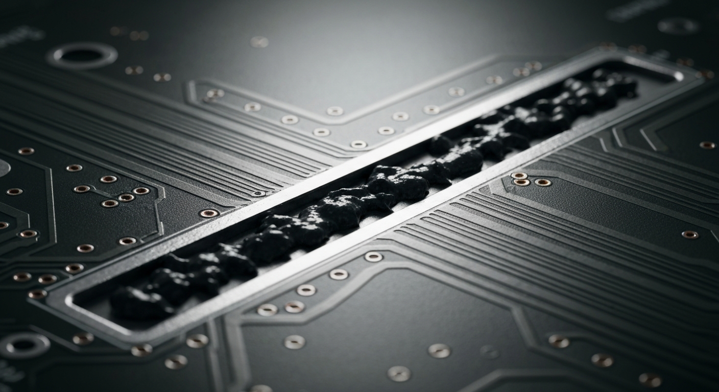
What is via tenting, plugging, and capping?
These methods control how vias are protected or sealed for soldering, routing, and assembly reliability.
Tenting covers the via with solder mask, plugging fills it partially or fully, and capping adds a plated copper layer over the filled via.
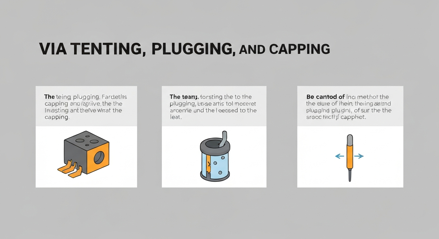
Deeper Insight
Tenting:
Via tenting uses solder mask to cover the via opening. It is cost-effective but not always reliable for fine-pitch designs. Mask may open during reflow, exposing the via.
Plugging:
Plugging fills the via with resin or solder mask. It prevents flux leakage, improves cleanliness, and protects the via from contamination. Plugging may be partial or full depending on design needs.
Capping (Via-in-Pad):
Capping occurs when the filled via is plated over with copper. This creates a flat SMT pad suitable for BGAs or fine-pitch ICs. Via-in-pad supports dense routing and excellent assembly stability but requires high manufacturing precision.
Factories follow IPC-4761 to categorize via protection levels. CAM teams adjust drilling parameters, resin viscosity, and plating cycle to avoid voids or pad collapse. B2B customers rely on these techniques when designing compact modules, multilayer HDI boards, or devices with strict assembly tolerances.
What is copper via filling (copper plug or electroplated fill)?
Copper filling provides the strongest via structure, supporting high current, thermal stability, and HDI stack-ups.
Copper via filling uses electroplated copper to completely fill vias, creating durable connections ideal for stacked or buried microvias.
Deeper Insight
Copper is the highest-performance filling material. Electroplating fills the via barrel with dense copper and then plates over to create a flat surface. This method is essential for:
- HDI stacked microvias
- High-power circuits
- Thermal vias under power ICs
- Complex multilayer boards requiring strong interconnects
Copper filling ensures excellent mechanical strength, which prevents cracks, delamination, and via fatigue. The plated structure also withstands repeated thermal cycling, making it suitable for industrial electronics, power modules, and RF devices.
Because copper filling requires advanced equipment and tight process control, only experienced manufacturers offer consistent results. Engineering teams analyze via aspect ratios, copper distribution, lamination sequence, and assembly requirements to ensure stable performance. This attention to detail supports both prototypes and mass-production orders in demanding applications.
How should designers choose the right via filling technique?
Different applications need different via treatments. The wrong choice can affect thermal performance, manufacturability, or assembly quality.
Designers choose the correct filling technique by evaluating layout density, component type, current flow, thermal requirements, and assembly method.
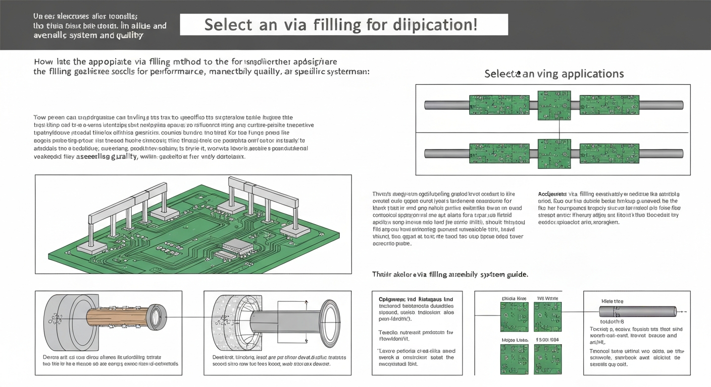
Deeper Insight
Selecting the right via filling method depends on several factors:
- BGA or fine-pitch ICs: Via-in-pad with copper or non-conductive filling
- Power circuits: Conductive paste or copper-filled vias
- Cost-sensitive projects: Standard tenting or plugging
- HDI multilayers: Copper-filled stacked microvias
- Thermal pads: Conductive or copper-filled vias for heat transfer
Manufacturers evaluate each design using DFM analysis. CAM engineers inspect via size, drill tolerances, aspect ratio, pad layout, and reflow conditions to recommend a suitable technique. For small-batch or prototype projects, choosing a method that balances cost and reliability helps avoid delays and redesigns.
Industries such as smart home devices, industrial controllers, and IoT modules benefit from optimized via filling because it improves soldering behavior, enhances thermal paths, and reduces long-term failures.
Conclusion
PCB via filling techniques play a critical role in reliability, assembly stability, and layout flexibility. By understanding methods such as non-conductive filling, conductive paste, tenting, plugging, capping, and copper via filling, designers can build stronger and more efficient circuits. An informed choice ensures clean SMT pads, stable thermal performance, and predictable long-term behavior across both prototypes and mass-production runs. Proper via filling supports high-density routing, improves BGA performance, and strengthens interlayer connections—making it essential for modern electronics across every industry.
