
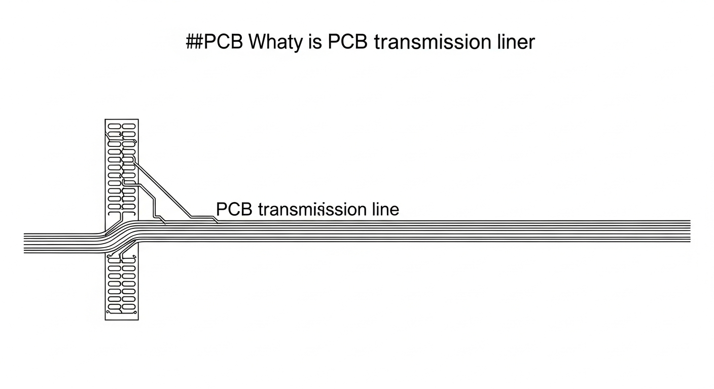
A PCB transmission line is a controlled-conductive path that carries high-speed signals across a printed circuit board while maintaining consistent impedance. It ensures stable, low-loss, and distortion-free signal propagation at high frequencies.
Transmission lines help prevent reflections, ringing, crosstalk, and signal degradation. They are essential for high-speed digital circuits, RF boards, and any design operating above a few hundred megahertz.
What exactly is a PCB transmission line?
When signals move fast, PCB traces behave like electromagnetic waveguides rather than simple wires. A transmission line controls this behavior.
A PCB transmission line is a trace engineered with specific geometry, layer structure, and dielectric properties to maintain a target impedance—often 50Ω or 90Ω—across the board.
Deeper Insight
A transmission line forms when a signal conductor and a reference plane work together to guide electromagnetic energy. Common structures include microstrip (outer layer), stripline (inner layer), and differential pairs.
Key parameters include:
- Trace width and thickness
- Dielectric height
- Copper roughness
- Solder mask influence
- Material dielectric constant (Dk)
These variables determine impedance, delay, and loss. Manufacturers use stack-up design, controlled etching, and precise lamination to achieve the specified geometry.
B2B OEM clients—especially those building IoT modules, routers, industrial controllers, or RF devices—depend on accurate transmission line design to ensure stable connectivity and reduce EMI problems. Engineering-driven factories provide impedance simulations and stack-up validation to prevent mismatch or signal distortion.
What types of PCB transmission lines are most common?
Different routing environments require different transmission line structures.
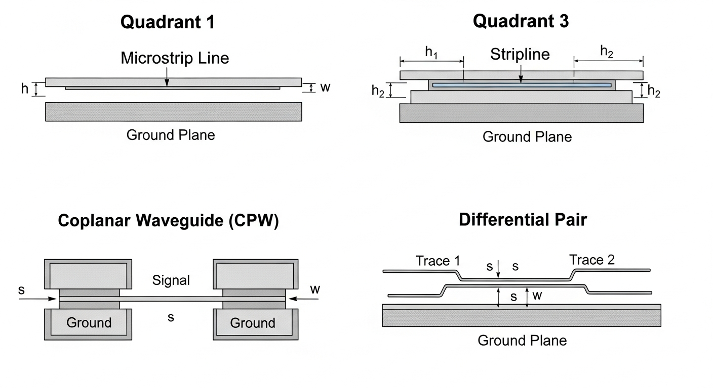
Common PCB transmission line types include microstrip, stripline, coplanar waveguide, and differential pairs.
Deeper Insight
1. Microstrip Line (External Layer)
- One trace above a ground plane
- Solder mask influences impedance
- Used for RF, Wi-Fi, Bluetooth, and antenna routing
2. Stripline (Inner Layer)
- Trace sandwiched between two ground planes
- Excellent noise isolation
- Used for high-speed digital buses
3. Coplanar Waveguide (CPW)
- Signal trace with ground on both sides
- Good for RF matching and antenna feedlines
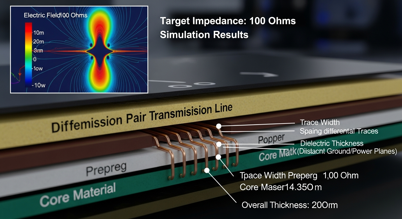
4. Differential Pairs
- Two traces carrying opposite signals
- Used for USB 3.x, PCIe, HDMI, LVDS, CAN, Ethernet
- Requires strict spacing and length matching
Manufacturers evaluate stack-up thickness, trace geometry, and dielectric loss to determine the correct structure. For IoT and industrial customers, transmission line selection affects RF accuracy, timing stability, and EMI performance.
Why is controlled impedance important for PCB transmission lines?
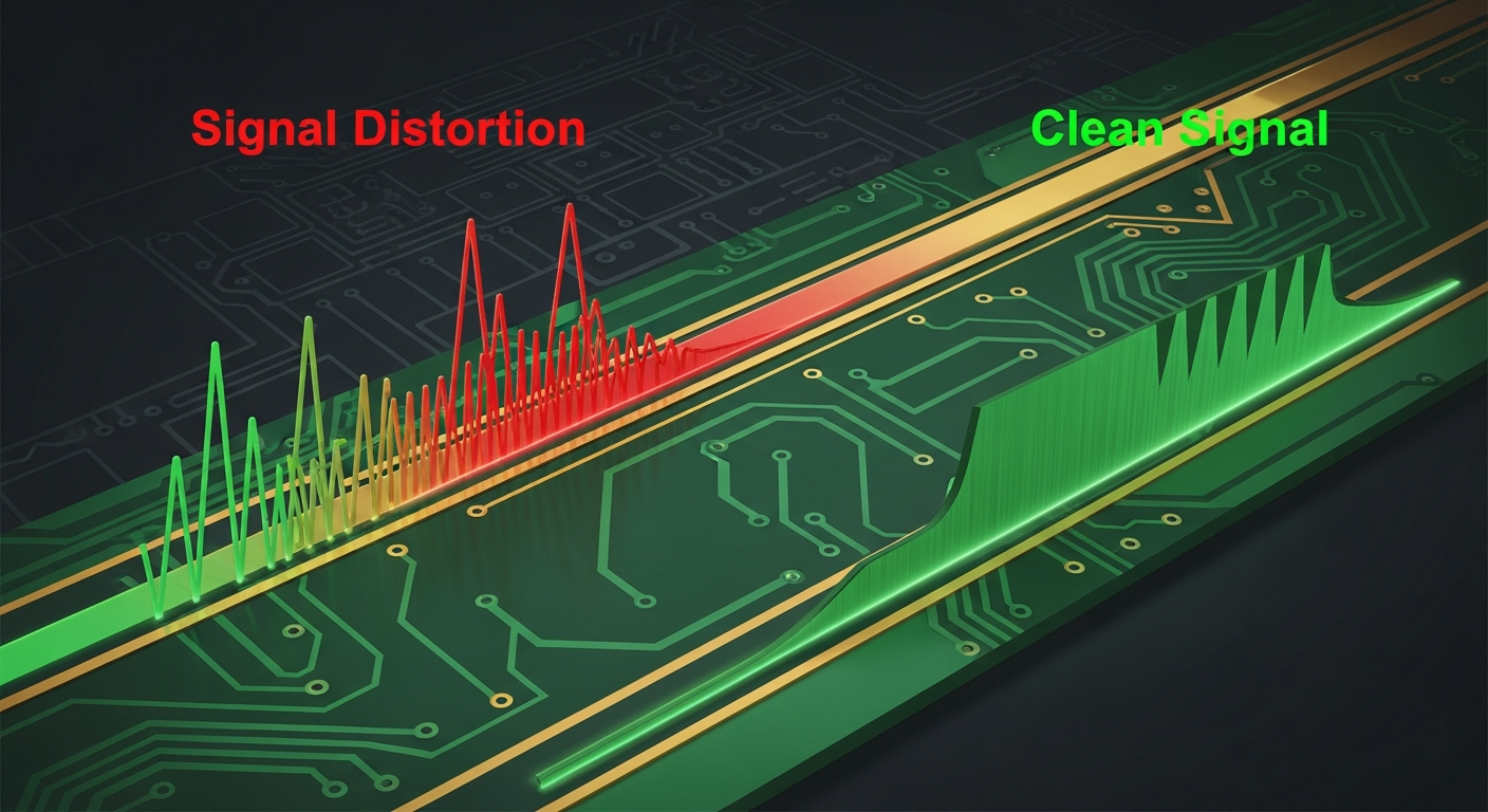
If impedance varies along a trace, the signal reflects, distorts, or loses strength.
Controlled impedance ensures that high-speed and RF signals travel cleanly without unexpected reflections or timing errors.
Deeper Insight
Impedance mismatch causes:
- Signal reflection
- Ringing and overshoot
- Eye-diagram closure
- Reduced switching margins
- Packet loss or communication failures
Transmission lines enforce a constant impedance value such as:
- 50Ω for RF and antenna traces
- 90Ω / 100Ω differential for USB, Ethernet, HDMI
- 85Ω differential for PCIe
Manufacturers achieve this through:
- Tight etching control
- Verified material Dk/Df specs
- Controlled lamination pressure and resin flow
- AOI and electrical impedance testing
OEM/ODM factories support designers with stack-up recommendations and pre-production impedance coupons to validate performance before full manufacturing.
How are PCB transmission lines designed?
Good transmission line design depends on geometry, layer choice, and accurate simulation.
Transmission lines are designed by setting target impedance, selecting a layer structure, and calculating trace width, spacing, and dielectric thickness.
Deeper Insight
Design steps typically include:
- Define target impedance based on interface requirements.
- Select stack-up containing material thickness, copper weight, and dielectric constants.
- Use impedance calculators to determine width, spacing, and trace geometry.
- Add ground references to stabilize return current paths.
- Apply length matching for differential or timing-critical signals.
- Avoid discontinuities such as sharp bends, via stubs, and abrupt width changes.
Manufacturers review the design during DFM analysis, correcting issues such as:
- Poor via transitions
- Inconsistent reference planes
- Impedance mismatches caused by solder mask
- Copper roughness inconsistencies
- Uneven differential spacing
These checks reduce signal integrity risks and improve product stability for industrial, telecom, and IoT customers.
Deeper Insight
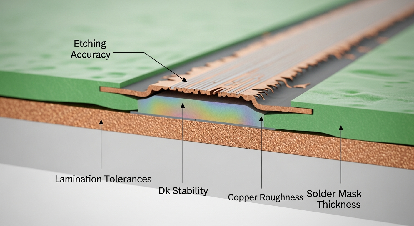
Critical manufacturing factors include:
1. Etching Precision
Small variations in trace width change impedance significantly.
2. Dielectric Thickness Tolerance
Incorrect spacing between trace and reference plane alters impedance.
3. Copper Roughness
Affects insertion loss and high-frequency attenuation.
4. Solder Mask Thickness
Modifies effective dielectric for microstrips.
5. Material Dk/Df Variation
Critical for RF, 5G, and high-speed digital systems.
Manufacturers control these factors using calibrated lamination, laser measurement, and impedance test coupons. For B2B buyers developing small-batch or mass projects, consistent material quality and precise stack-up replication ensure predictable electrical performance in every production batch.
Conclusion
A PCB transmission line is a carefully engineered trace that controls impedance and supports clean high-speed or RF signal propagation. By using structures like microstrip, stripline, and differential pairs, and by applying correct design rules and stack-up planning, engineers maintain signal quality and prevent reflection or loss. Manufacturing precision—etching, material choice, lamination control—plays an equally important role. With proper engineering collaboration and accurate production processes, transmission lines deliver stable, reliable performance from prototype to mass production across advanced electronics and IoT systems.
