
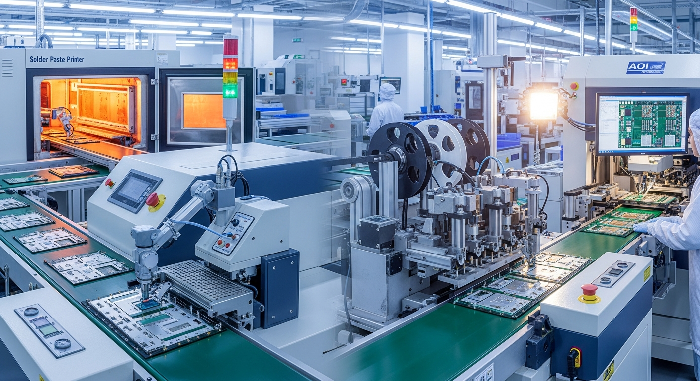
PCBA manufacturing transforms a bare PCB into a fully assembled, functional electronic module through soldering, inspection, and testing.
A clear understanding of the PCBA workflow helps engineering teams reduce design risks, avoid assembly delays, and achieve predictable results from prototype to mass production.
What are the main stages of the PCBA manufacturing process?
Many project delays come from unclear workflows, missing files, or assembly rules that do not match real factory capabilities.
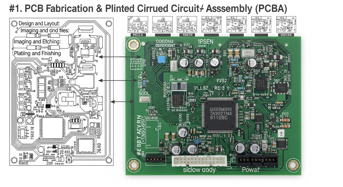
The PCBA process includes PCB fabrication, SMT assembly, DIP soldering, inspection, and final functional testing.
From Bare Board to Fully Assembled Module
The full process starts with confirmed Gerber and BOM files. PCB fabrication prepares copper layers, solder mask, and surface finishes. SMT assembly places surface-mount components using automated pick-and-place systems. Reflow soldering forms joints, followed by DIP plugging for through-hole parts. AOI, X-ray, ICT, and FCT verify electrical and mechanical correctness before final packaging.
In B2B hardware projects, mismatched footprints, missing paste layers, or unstable supply chains often disrupt schedules. Factories with engineering-driven workflows review design files, optimize BOM sourcing, and align PCB fabrication with SMT rules. With in-house production, quality remains consistent across prototype and volume batches.
How does SMT assembly work in the PCBA process?
Incorrect solder volume or misalignment often causes tombstoning, bridges, or poor electrical contact.
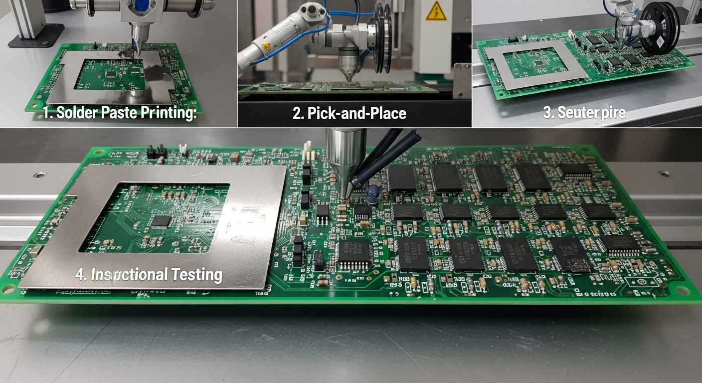
SMT assembly automates component placement using solder paste printing, pick-and-place, and reflow soldering.

Stencil Printing, Component Placement, and Reflow
SMT begins with applying solder paste through a stainless-steel stencil. Pick-and-place machines place resistors, capacitors, ICs, and RF modules with precise alignment. The board enters a reflow oven where solder melts, wets, and forms strong connections. Temperature profiles must suit component density, package type, and board thickness.
In real production, issues such as stencil wear, incorrect pad design, or poor thermal balance often lead to weak solder joints. Engineering-led factories optimize stencil apertures, verify paste performance, and adjust reflow settings. AOI systems check alignment, joint shape, and polarity, catching issues early and smoothing the transition to small-batch and larger-volume runs.
How does DIP or through-hole soldering support high-power or mechanical components?
Surface-mount alone cannot handle high current, mechanical stress, or connector durability.
DIP soldering secures large components by inserting leads through the PCB and forming strong barrel joints.
Wave Soldering, Manual Plug-In, and Mechanical Strength
Through-hole parts such as transformers, connectors, relays, and high-power resistors often require hand insertion followed by wave soldering. A molten solder wave fills plated holes, forming strong joints capable of handling vibration, load cycles, and thermal stress.
In B2B applications, incorrect hole ratios, pad sizes, or thermal distribution often cause solder voids or incomplete fill. Engineering-based factories check drill tolerances, optimize hole-to-pin fit, and confirm plating thickness. With IPC-A-610 and RoHS processes in place, through-hole assembly achieves consistent strength across all production batches.
What inspection methods ensure the quality of assembled PCBA boards?
Undetected defects create field failures, unstable performance, or costly returns.
PCBA quality is verified using AOI, X-ray, ICT, and functional testing.

Automated Optical, X-Ray, and Electrical Testing
AOI inspects solder joints, component orientation, and marking accuracy. X-ray verifies hidden structures such as BGA balls or voids. ICT checks resistances, capacitances, and continuity through test points. FCT simulates real operating conditions to verify system functionality.
Across commercial projects, factories with complete inspection workflows reduce risk and improve yield. When design, PCB fabrication, and SMT operate under unified engineering standards, test coverage becomes stronger and more consistent. This leads to stable, repeatable quality from early prototypes to mass production.
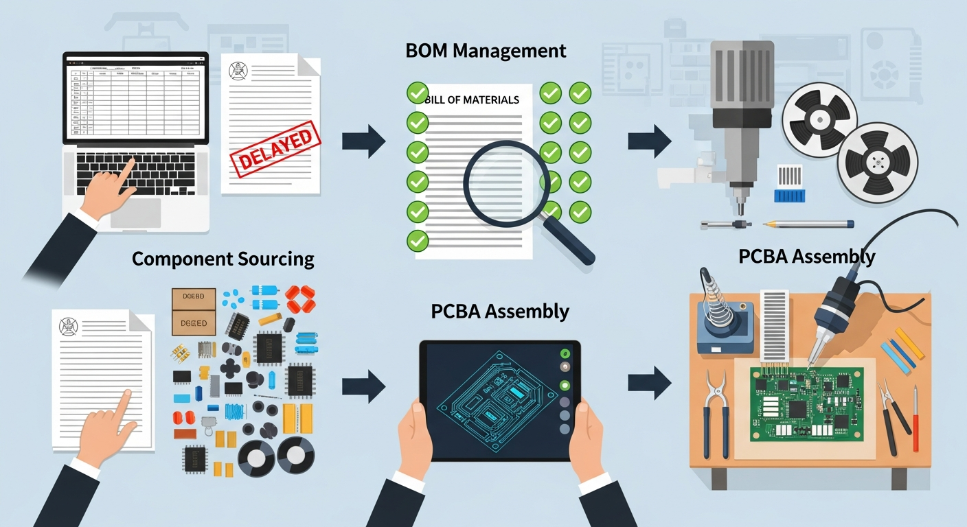
How does BOM management affect the PCBA workflow?
Poor component sourcing causes delays, cost increases, or design revisions.
Effective BOM management ensures component availability, compatibility, and production stability.
Sourcing, Substitution, and Supply-Chain Stability
Correct BOM management involves verifying part numbers, checking package types, validating footprints, and ensuring long-term availability. Alternate components may be introduced to reduce cost or avoid shortages, but electrical and mechanical compatibility must remain intact.
Factories with their own procurement and engineering teams review BOM lists, suggest reliable substitutes, and prevent mismatches between design intent and assembly reality. With strong supplier networks, lead times become predictable and cost control becomes easier throughout the entire production cycle.
How does the PCBA process support reliable product testing and final assembly?
Inadequate testing often leads to inconsistent performance or product instability after shipping.
The PCBA process includes final quality checks that ensure each board is ready for enclosure assembly and field use.
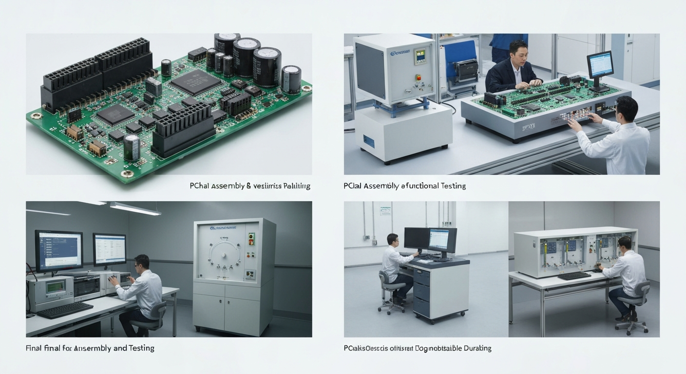
End-of-Line Inspection, Burn-In, and System-Level Validation
After electrical tests, boards may undergo burn-in or environmental simulation to identify hidden weaknesses. Connectors, sensors, displays, and power modules undergo functional verification to confirm correct operation. Packaging and labeling follow standardized procedures to support traceability.
Factories with end-to-end capabilities provide complete testing documentation, process control logs, and traceable serial data. This reduces warranty claims, builds customer confidence, and supports long-term reliability, especially for industrial, medical, and IoT applications.
Conclusion
The PCBA manufacturing process integrates PCB fabrication, SMT assembly, DIP soldering, inspection, and functional verification into a structured workflow. Each stage influences electrical performance, mechanical stability, and long-term reliability. With engineering-driven practices, in-house SMT lines, BOM optimization, and complete testing systems, production becomes predictable from prototypes to mass shipments. This level of consistency strengthens product quality, shortens development cycles, and supports the long-term success of industrial, IoT, automotive, and consumer electronics across global markets.
