
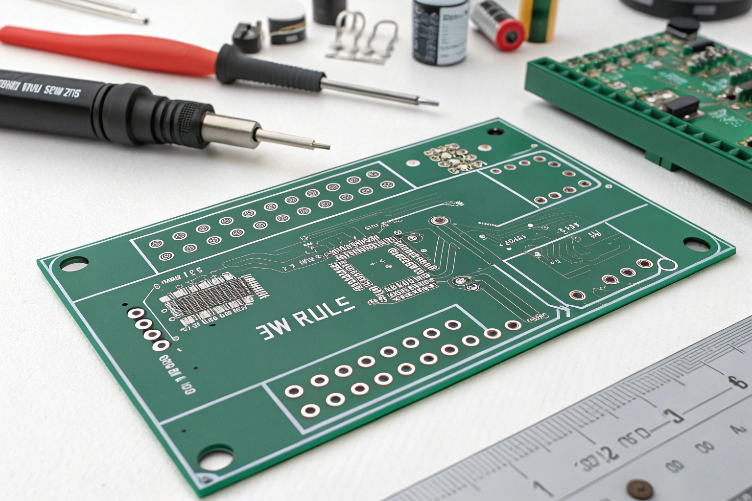
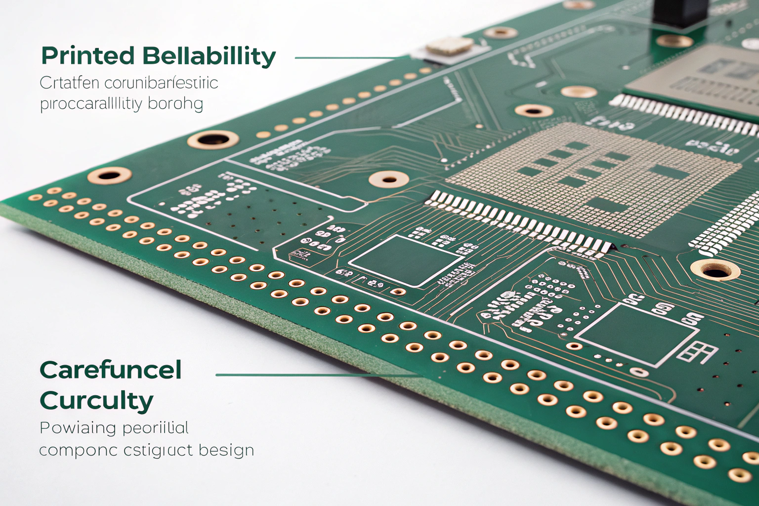
The 3W rule is a fundamental layout guideline in PCB design that defines minimum spacing between signal traces to reduce crosstalk and signal interference. It states that the distance between two adjacent traces should be at least three times the trace width.
In practical manufacturing and assembly, the 3W rule is not only a design concept but also a key reference for process stability, signal integrity, and yield control. When PCB design aligns with manufacturing capability, downstream PCBA processes become more stable and predictable.
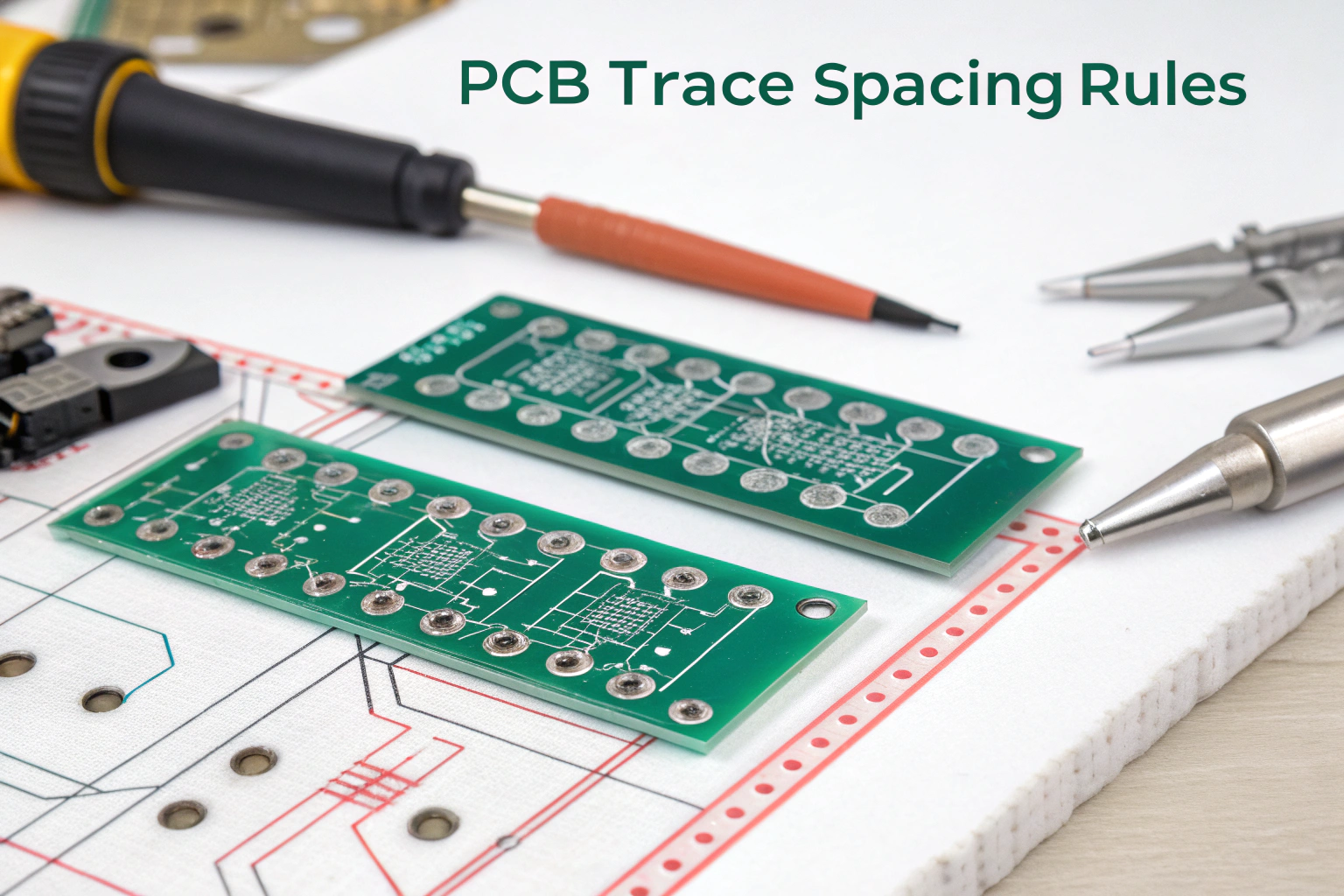
Why does the 3W rule matter in PCB layout?
High-speed and high-density PCB designs are increasingly sensitive to noise and signal coupling. Without proper spacing, adjacent traces can interfere with each other through capacitive and inductive coupling.
The 3W rule provides a simple and effective spacing benchmark. If a trace width is 6 mil, the recommended spacing to the next parallel trace should be at least 18 mil. This reduces electromagnetic coupling and helps maintain signal clarity.
From a manufacturing standpoint, designs that follow the 3W rule are more tolerant to etching variations and solder mask alignment shifts. This directly improves PCB consistency and reduces the risk of hidden electrical issues after assembly.
How does the 3W rule reduce crosstalk and noise?
Crosstalk occurs when electromagnetic fields from one signal trace affect a neighboring trace. This issue becomes more severe with high-speed signals, long parallel routing, and narrow spacing.
By increasing the spacing to three times the trace width, the coupling capacitance between traces drops significantly. This spacing acts as a buffer zone that weakens interference paths.
In real production, reduced crosstalk translates to fewer functional test failures and more stable electrical performance. Boards that respect spacing rules show higher pass rates during functional testing, especially in communication, control, and mixed-signal designs.
Is the 3W rule always mandatory?
The 3W rule is a guideline, not an absolute law. In compact or high-density designs, it may not always be achievable.
When spacing is limited, other methods can compensate, such as ground shielding traces, differential pair routing, or controlled impedance structures. However, these solutions increase design complexity and manufacturing demands.
From a factory perspective, designs that violate spacing guidelines require tighter process windows. This includes stricter etching control, more accurate solder mask registration, and increased inspection effort. Following the 3W rule wherever possible simplifies production and improves long-term reliability.
How does the 3W rule impact PCB fabrication?
PCB fabrication accuracy is directly affected by trace width and spacing.
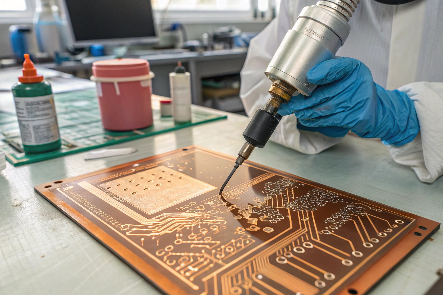
During etching, copper removal is influenced by chemical balance, temperature, and time. Narrow spacing increases the risk of over-etching, under-etching, or residual copper bridges.
Designs that follow the 3W rule provide sufficient margin for fabrication variations. This improves yield, especially for multi-layer boards and fine-line designs. Stable spacing also ensures better solder mask coverage between traces, reducing solder bridging during assembly.
For manufacturers with in-house PCB capability or long-term fabrication partners, spacing-friendly designs reduce rejection rates and improve delivery consistency.
How does the 3W rule affect PCBA assembly quality?
PCB design decisions directly influence PCBA assembly outcomes.
Adequate trace spacing improves solder mask integrity between pads and traces. This lowers the risk of solder bridging during reflow soldering, especially for fine-pitch components and dense layouts.
In SMT workshops, boards with proper spacing show more stable solder paste printing results. Solder paste is less likely to spread across unintended areas, and AOI detection becomes more accurate.
From an assembly engineering view, respecting spacing rules reduces rework, manual touch-up, and inspection pressure. This leads to smoother line operation and higher first-pass yield.
How do factory workshops evaluate spacing during production?
Professional manufacturing environments include multiple checkpoints to evaluate spacing-related risks.

Engineering teams review Gerber data during DFM analysis, checking trace width, spacing, and solder mask openings. Any areas below process capability limits are flagged before production starts.
On the shop floor, AOI systems monitor solder bridging risks that may arise from tight spacing. Process engineers adjust stencil design and reflow profiles to match board characteristics.
Factories with mature process control systems treat spacing not as a design-only issue, but as a cross-functional parameter connecting design, fabrication, and assembly.
How does the 3W rule support long-term product reliability?
Spacing is not only about initial performance but also about durability.
Boards with insufficient spacing are more vulnerable to contamination, humidity, and thermal expansion. Over time, these factors can cause leakage currents or intermittent faults.
Following the 3W rule improves insulation resistance and reduces long-term electrical stress. This is especially important for industrial, energy, and control electronics that operate continuously in demanding environments.
From a manufacturing quality perspective, designs with proper spacing show fewer field returns and more stable lifecycle performance.
Conclusion
The 3W rule is a simple but powerful principle in PCB design that connects electrical performance with manufacturing reality. By maintaining trace spacing at three times the trace width, crosstalk is reduced, fabrication yield improves, and assembly quality becomes more stable.
For manufacturers, spacing-friendly designs lower process risk, simplify workshop control, and support consistent quality from early builds to long-term production. When PCB layout respects the 3W rule, the entire manufacturing flow benefits—from fabrication and SMT assembly to testing, reliability, and final product performance.
