
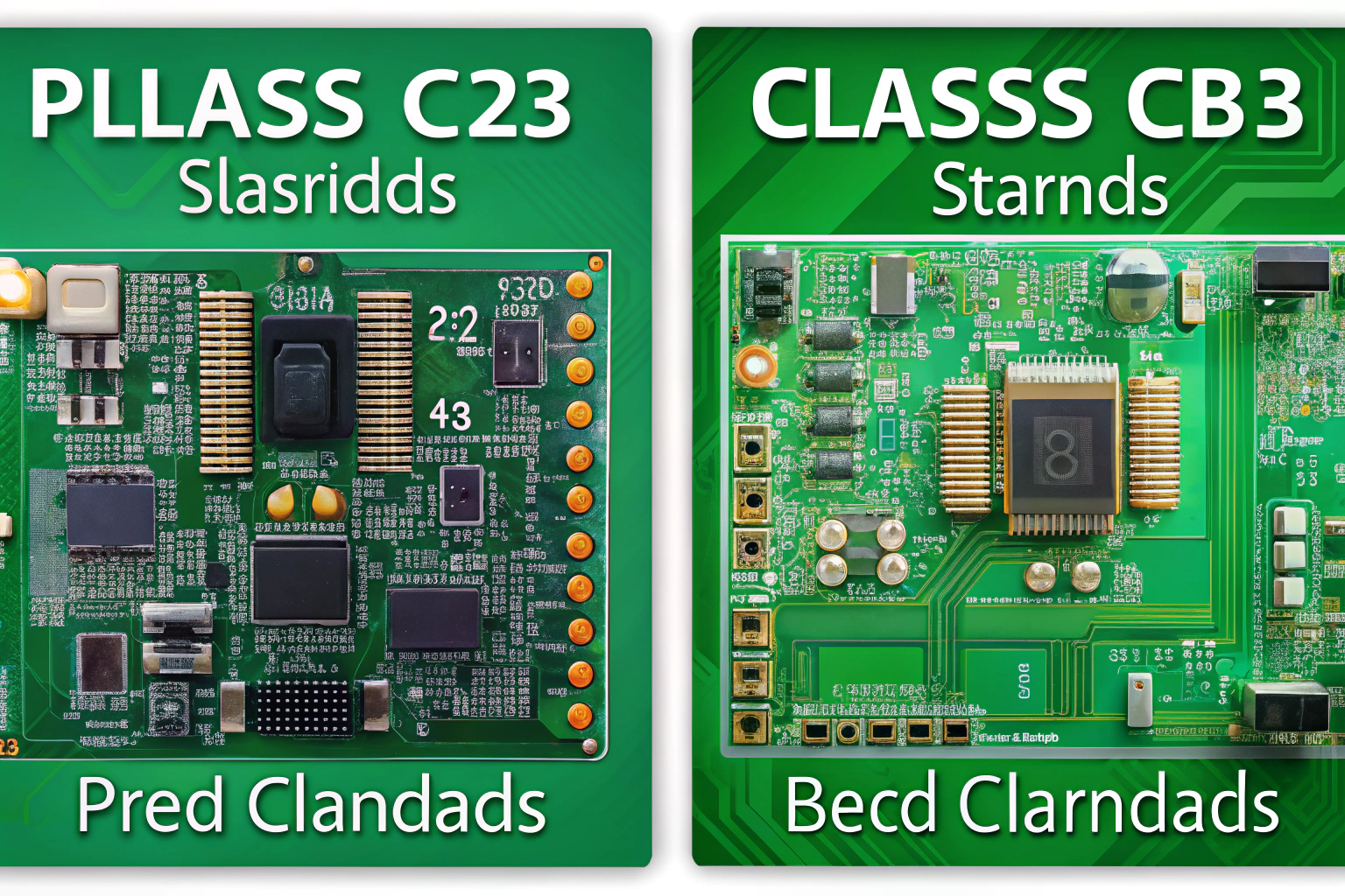
Class 2 and Class 3 PCBs are quality classifications defined by IPC standards to describe different levels of reliability and inspection requirements in printed circuit board manufacturing. These classes guide material selection, process control, inspection criteria, and long-term performance expectations.
In manufacturing practice, the difference between Class 2 and Class 3 PCBs is not only about inspection tolerance. It reflects a completely different mindset in process control, workshop discipline, and reliability assurance.
How are Class 2 and Class 3 PCBs defined?
Class 2 PCBs are designed for dedicated service electronic products. These products require stable performance and extended life, but occasional downtime or repair is acceptable.

Class 3 PCBs are designed for high-reliability electronic products. Continuous operation, harsh environments, and zero-tolerance for failure are typical requirements.
From a manufacturing viewpoint, Class 3 represents the highest standard. Every process step, from material control to final inspection, must meet stricter limits compared to Class 2.
What are the key quality differences between Class 2 and Class 3?
The main differences lie in allowable defects and acceptance criteria.
Class 2 allows limited cosmetic imperfections and minor process variations as long as electrical function is not affected. Annular ring reduction, solder mask misalignment, and surface marks have wider tolerance windows.
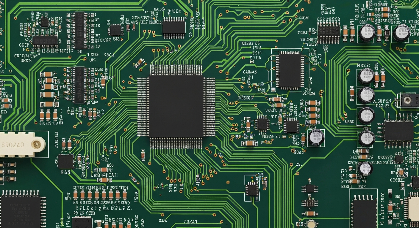
Class 3 imposes much tighter limits. Annular rings must be larger, copper thickness more uniform, and solder joints fully wetted with minimal voiding.
In production, this means Class 3 boards require higher process stability and more frequent inspection checkpoints to prevent borderline defects.
How does PCB fabrication differ for Class 2 and Class 3?
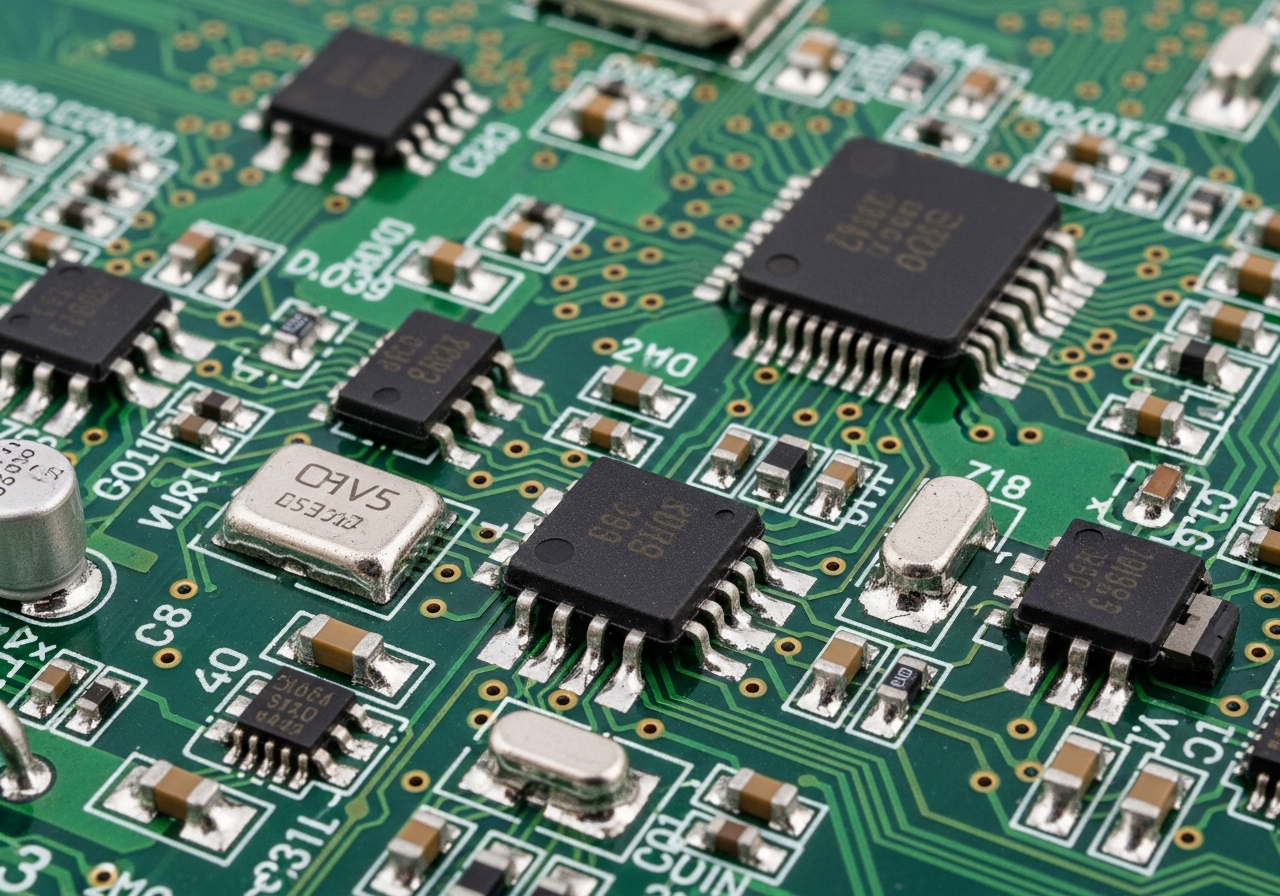
Fabrication processes follow the same general flow, but execution standards differ significantly.
For Class 2 PCBs, standard laminates, drilling accuracy, and plating thickness are typically sufficient. Process capability focuses on efficiency and consistency.
For Class 3 PCBs, material selection often shifts to higher-grade laminates with better thermal stability. Drilling parameters are optimized to reduce smear and wall roughness. Copper plating thickness is increased to improve via reliability.
Factories producing Class 3 PCBs operate with narrower process windows and higher scrap control to ensure every board meets specification.
How does PCBA assembly change between Class 2 and Class 3?
Assembly requirements become more demanding when moving from Class 2 to Class 3.
Class 2 PCBA focuses on correct placement, functional solder joints, and electrical performance. Minor solder fillet variations may be acceptable.
Class 3 PCBA requires uniform solder fillets, full wetting, controlled void percentages, and stricter cleanliness standards. Reflow profiles are tightly controlled, and manual soldering follows documented workmanship criteria.
These requirements increase assembly time and inspection effort but significantly reduce long-term failure risk.
How do factory workshops support Class 3 production?
Workshop environment plays a major role in meeting Class 3 standards.
Class 3 production areas typically feature tighter temperature and humidity control, enhanced ESD protection, and stricter material handling rules. Operators receive additional training and certification.

Process records are more detailed, and traceability is maintained from raw materials to finished boards. Any deviation triggers immediate corrective action.
This level of discipline ensures repeatability and consistency across production batches.
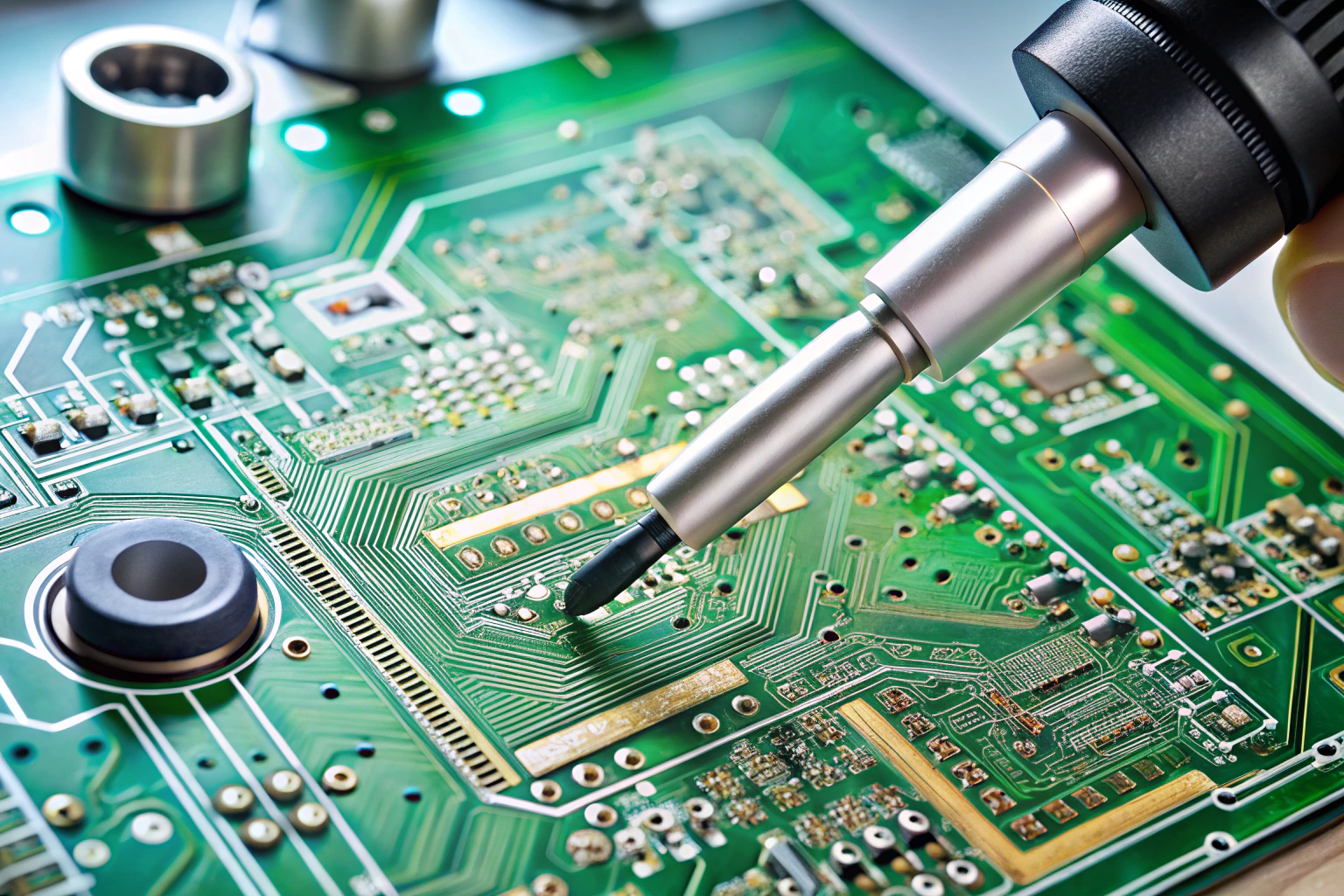
What inspection and testing differences exist?
Inspection intensity increases significantly from Class 2 to Class 3.
Class 2 typically uses AOI and electrical testing as primary verification methods. Sampling inspection may be applied for certain characteristics.
Class 3 often requires 100% inspection for critical features. X-ray inspection, microsection analysis, and enhanced electrical testing are more commonly applied.
These inspections confirm structural integrity, solder joint reliability, and long-term durability.
Where are Class 2 and Class 3 PCBs commonly used?
Class 2 PCBs are widely used in industrial equipment, control systems, and professional electronics where stable operation is required but controlled downtime is acceptable.
Class 3 PCBs are used in mission-critical systems such as aerospace electronics, medical life-support devices, transportation control systems, and energy infrastructure.
In these environments, failure consequences define the class selection more than cost or complexity.
Conclusion
Class 2 and Class 3 PCBs represent two distinct reliability levels in electronic manufacturing. Class 2 balances performance and manufacturability for stable, long-life products. Class 3 focuses on maximum reliability, demanding stricter materials, tighter processes, and comprehensive inspection.
From fabrication to assembly and testing, Class 3 production requires disciplined factory management, advanced process control, and experienced engineering support. When these standards are fully implemented, the resulting PCBs deliver exceptional durability and consistent performance throughout demanding operational lifecycles.
