
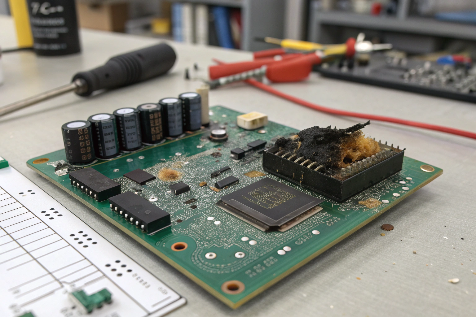
The main cause of PCB failure is poor solder joint reliability, usually triggered by thermal stress, improper process control, or material mismatch. Most PCB failures do not come from circuit design alone, but from how the board is manufactured, assembled, and stressed over time.
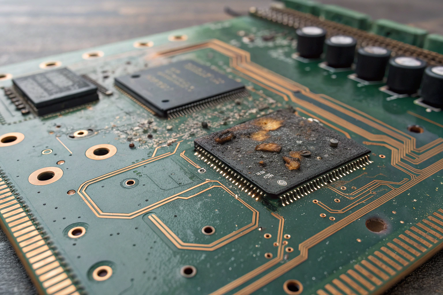
PCB failure is rarely sudden. It is usually the final result of small defects introduced during production that grow under heat, vibration, and long-term use.
In electronics manufacturing, understanding the true root causes of PCB failure is essential for improving yield, reducing returns, and ensuring long-term product stability.
Why Solder Joint Failure Is the Most Common PCB Failure Mode?
Solder joints are the weakest physical link.
They fail before copper traces or components.

A PCB may contain hundreds or thousands of solder joints. Each joint experiences thermal expansion, contraction, and sometimes mechanical stress. If even one critical joint fails, the entire board can stop functioning.
Common solder joint failure mechanisms include:
- Cold or insufficient solder joints
- Micro-cracks caused by thermal cycling
- Poor wetting due to oxidation or contamination
- Excessive intermetallic growth
These issues often originate during reflow or wave soldering. Incorrect temperature profiles, uneven heating, or unstable solder paste behavior create joints that look acceptable but lack long-term strength.
In manufacturing workshops, solder joint reliability is controlled through thermal profiling, paste inspection, and strict process windows. Without these controls, failure rates increase dramatically after products enter real-world use.
How Thermal Stress Drives PCB Failure Over Time?
Heat is unavoidable in electronic products.
Uncontrolled heat accelerates failure.
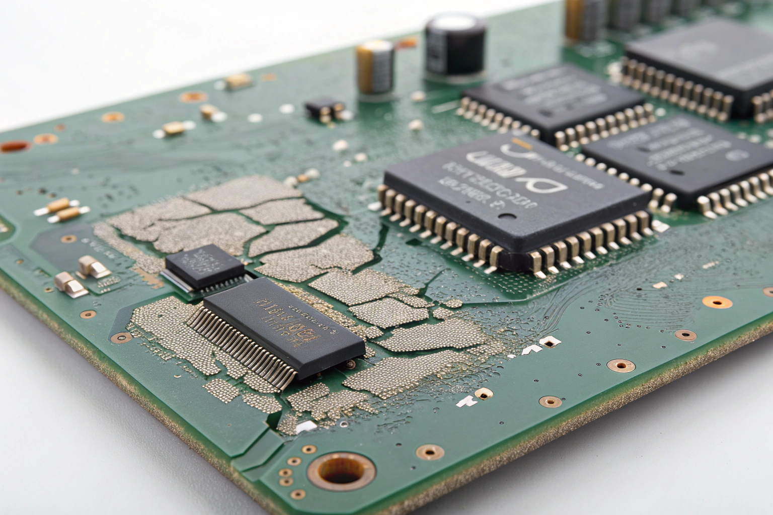
Every PCB expands when heated and contracts when cooled. Different materials expand at different rates. Copper, solder, laminate, and components all react differently to temperature change.
Repeated thermal cycling causes:
- Fatigue cracks in solder joints
- Pad lifting from the laminate
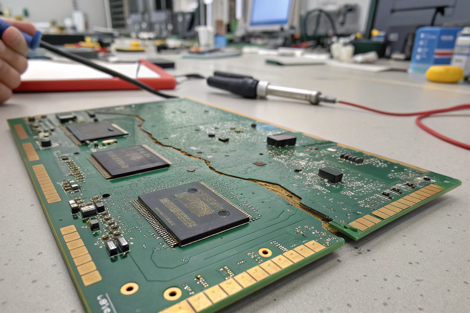
- Delamination between PCB layers
- Via cracking in multilayer boards
High-power components, poor heat dissipation, and aggressive operating environments amplify these effects.
In professional manufacturing, thermal stress is addressed through material selection, board stack-up design, and controlled soldering profiles. Heat sinks, thermal vias, and balanced copper distribution reduce localized stress.
Ignoring thermal behavior during manufacturing leads to early-life or mid-life PCB failure.
Why Poor Process Control Causes Hidden PCB Defects?
Most PCB failures are invisible at first.
They originate from process variation.
Lack of process discipline introduces variation that accumulates into failure risk. Small deviations during assembly may not stop the board from working initially, but they shorten its usable life.
Typical process-related causes include:
- Inconsistent solder paste volume
- Unverified reflow profiles
- Manual temperature adjustments
- Skipped equipment calibration
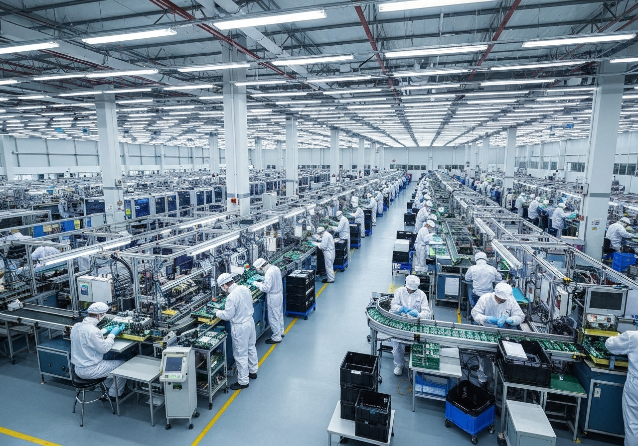
In factory workshops, every step is interconnected. A small issue at printing or placement affects soldering quality downstream.
High-quality manufacturers rely on SPI, AOI, and process data tracking to catch problems early. When these systems are missing or ignored, PCB failures appear later in the field instead of on the production line.
How Material Quality Directly Impacts PCB Reliability?
Not all PCB materials behave the same.
Low-quality materials fail faster.
PCB failure is often traced back to material choices made to reduce cost. Low-Tg laminates, poor copper adhesion, and unstable surface finishes reduce thermal and mechanical durability.
Material-related failure risks include:
- Early delamination under heat
- Poor solderability due to surface oxidation
- Weak pad adhesion leading to pad lift
- Increased moisture absorption
In manufacturing, incoming material inspection and supplier control are critical. PCB finishes such as ENIG, OSP, or HASL must match assembly and operating requirements.
Material shortcuts may pass initial testing but show high failure rates after months of operation.
Why Design-for-Manufacturing Issues Cause PCB Failure?
A working design is not always manufacturable.
Manufacturing limits matter.
Designs that ignore manufacturing realities increase failure risk. Tight pad spacing, unbalanced copper areas, and poor via placement create uneven heating and stress concentration.
Common DFM-related failure causes include:
- Tombstoning and uneven solder joints
- Incomplete reflow under large components
- Via-in-pad defects without proper filling
- Signal integrity degradation after rework
In professional workflows, DFM review happens before production. Engineers analyze thermal balance, solderability, and assembly risk.
Skipping this step pushes problems into production, where fixes are expensive and reliability suffers.
How Workshop Environment Affects PCB Failure Rates?
Environment shapes process stability.
Small changes have big impact.
Humidity, temperature, and cleanliness directly influence PCB assembly quality. Excess moisture leads to solder balling, voids, and popcorning in components.
In controlled workshops:
- Humidity is monitored and limited
- Moisture-sensitive components are baked
- PCBs are stored in dry cabinets
- ESD protection prevents latent damage
Without environmental control, even well-designed processes produce unstable results. These hidden defects often appear as intermittent failures that are difficult to diagnose.
Why Electrical Overstress Is a Secondary but Serious Cause?
Electrical stress accelerates existing weaknesses.
It rarely acts alone.
Overvoltage, current spikes, and poor grounding can damage components and traces. However, these failures often exploit pre-existing weaknesses such as marginal solder joints or thin copper.
Manufacturing quality determines how much electrical stress a PCB can tolerate. Strong joints and clean layouts resist damage better than marginal ones.
This is why electrical failure analysis often points back to manufacturing quality rather than usage alone.
Conclusion
The main cause of PCB failure is poor solder joint reliability, driven by thermal stress, weak process control, material limitations, and manufacturing variation. Most PCB failures are not caused by a single mistake, but by a chain of small issues introduced during assembly and amplified during real-world operation. Professional manufacturing focuses on stable soldering processes, disciplined workshop control, proper material selection, and early DFM review to prevent these failures before they leave the factory. When these fundamentals are respected, PCB reliability improves dramatically, field failures drop, and product lifespans extend far beyond initial expectations.
