
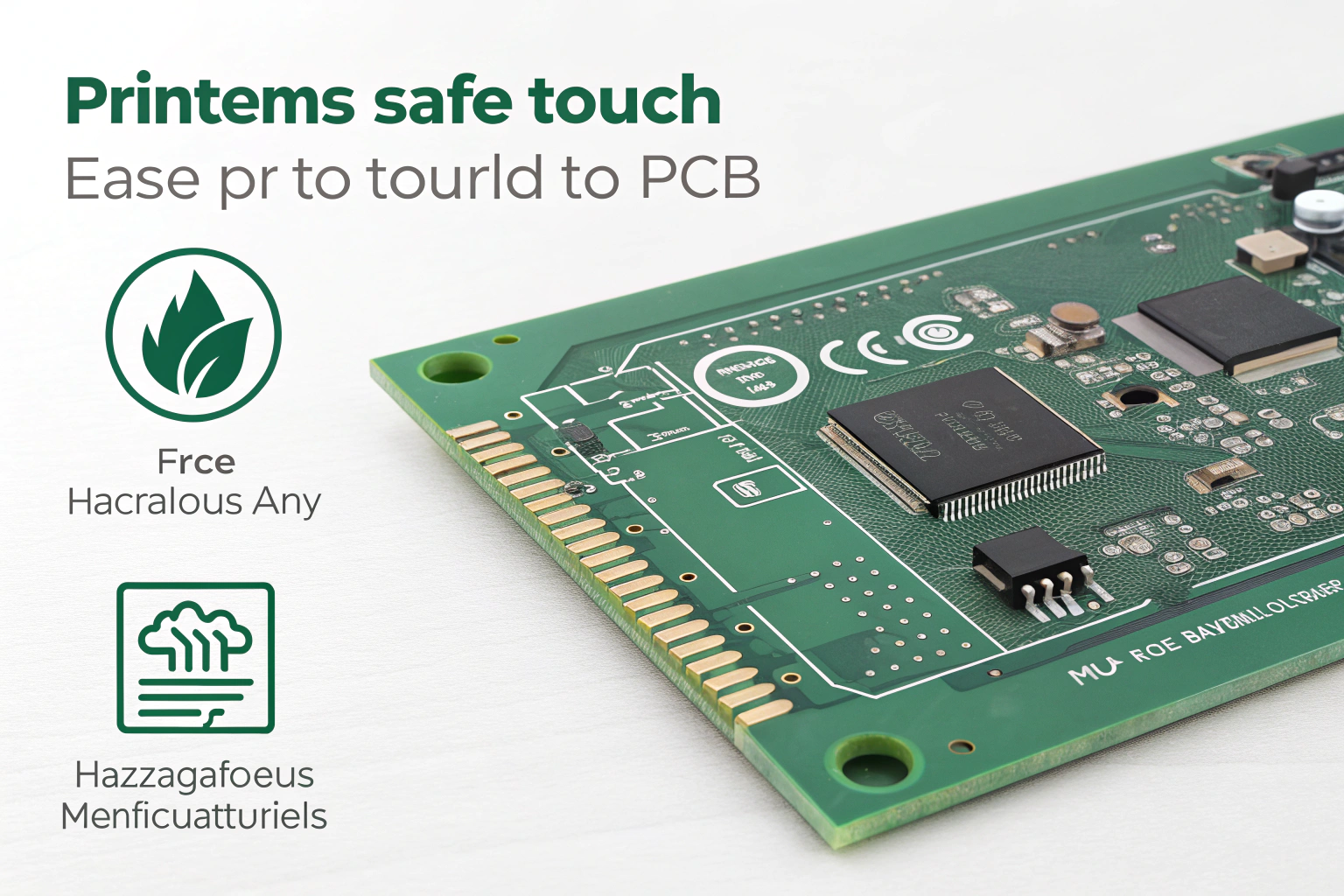
PCBs are generally safe to touch from a human health perspective, but touching them is not safe for the PCB itself in many situations. Direct contact can introduce electrostatic discharge, moisture, oils, and mechanical stress that reduce reliability and lifespan.
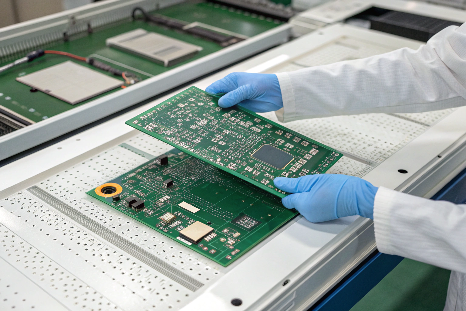
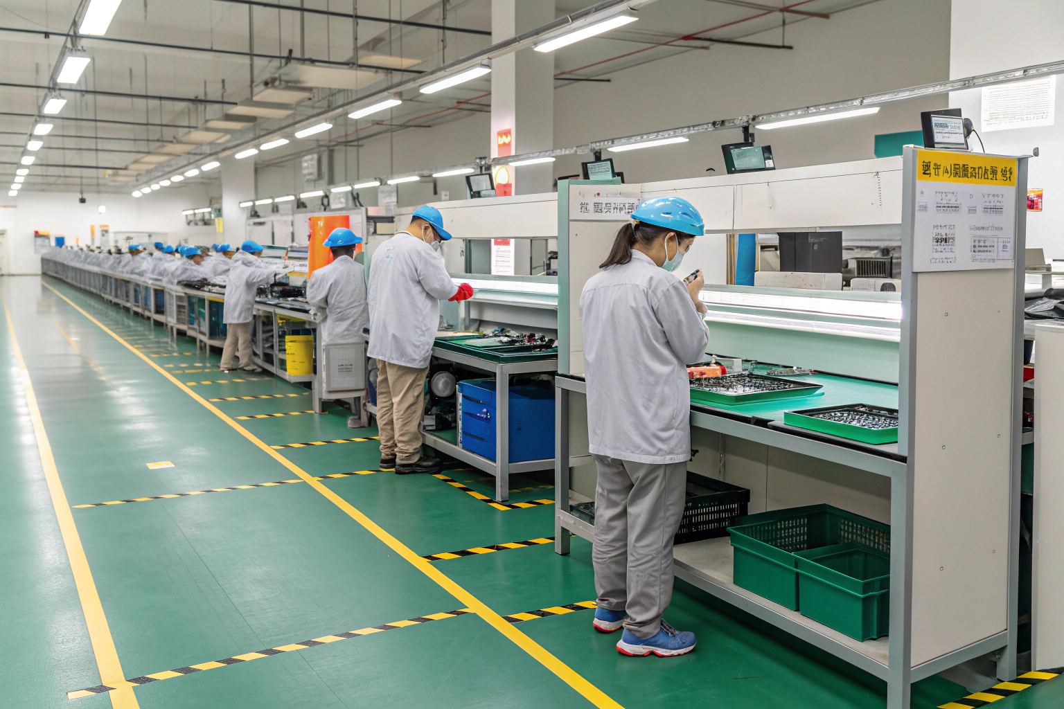
In electronics manufacturing, PCB handling is treated as a controlled process, not a casual action.
Understanding PCB safety requires separating human safety from product reliability.
PCBs Are Not Dangerous to Humans Under Normal Conditions
Bare PCBs do not pose an immediate hazard.
There is no inherent toxicity or shock risk.
A powered-off PCB made with standard materials such as FR4, copper, and solder mask is not harmful to human skin. There are no exposed chemicals that cause instant injury, and static contact alone does not create electric shock.
However, this does not mean unrestricted handling is acceptable. While human safety is not the concern, product integrity is.
In manufacturing environments, the goal is not to protect people from PCBs, but to protect PCBs from people.
Electrostatic Discharge Is the Primary Risk When Touching PCBs
Static electricity causes invisible damage.
Failure often appears much later.
Electrostatic discharge (ESD) occurs when static charge transfers from the body to electronic components. Sensitive devices such as ICs, MOSFETs, and sensors can be damaged by voltages far below what humans can feel.
ESD damage may not cause immediate failure. Instead, it weakens internal semiconductor structures, leading to:
- Early-life failure
- Intermittent behavior
- Reduced long-term reliability
In factory workshops, ESD control is mandatory. Grounded workstations, wrist straps, conductive floors, and anti-static tools are standard. Bare-hand contact is avoided not because it is unsafe for people, but because it is unsafe for the electronics.
Skin Oils and Moisture Create Long-Term PCB Damage
Touching a PCB leaves contamination behind.
Damage develops slowly over time.
Human skin transfers oils, salts, and moisture onto PCB surfaces. These residues attract humidity from the air and reduce surface insulation resistance.
Over time, this leads to:
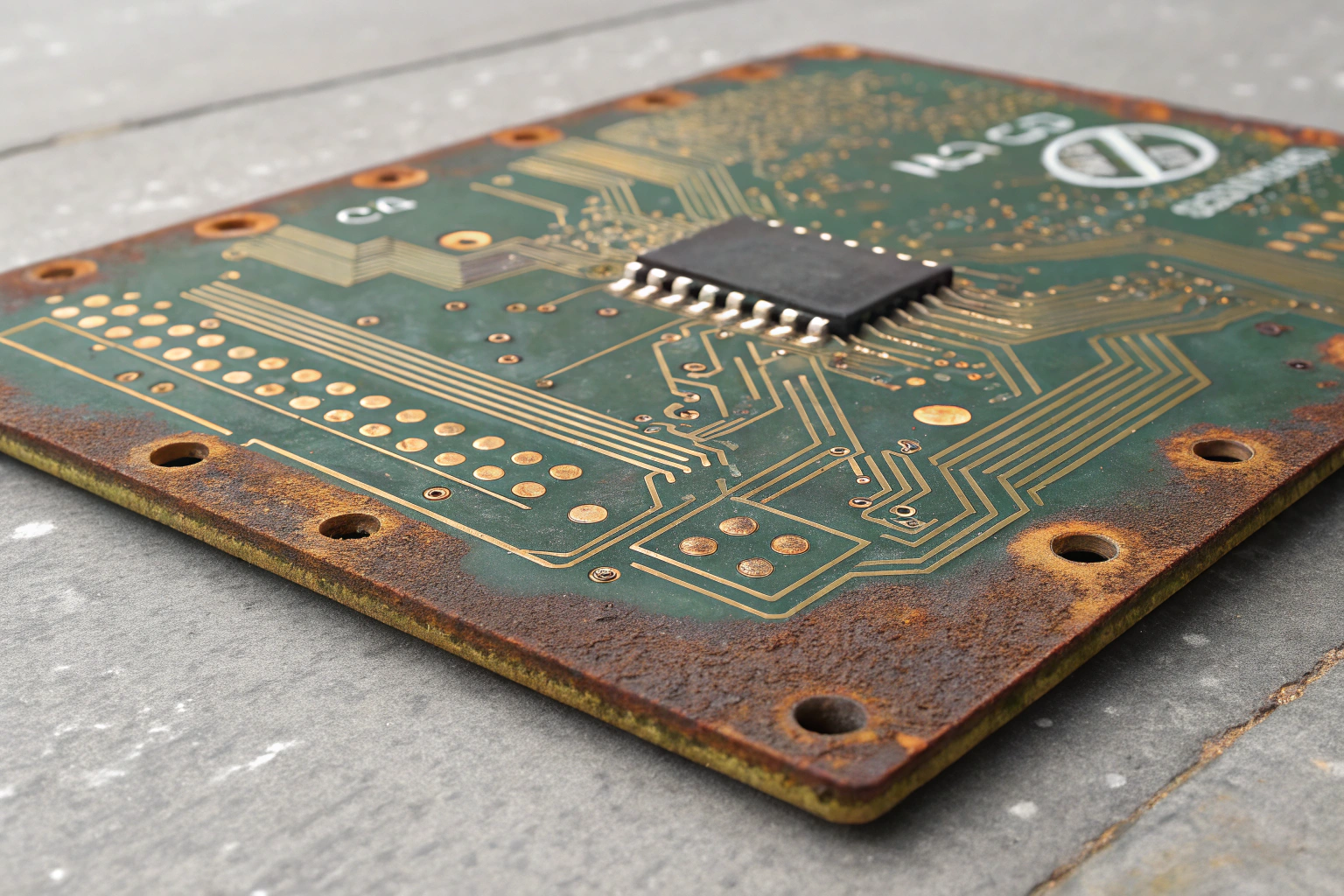
- Corrosion of copper and component leads
- Leakage currents between fine-pitch pads
- Degraded solder joint reliability
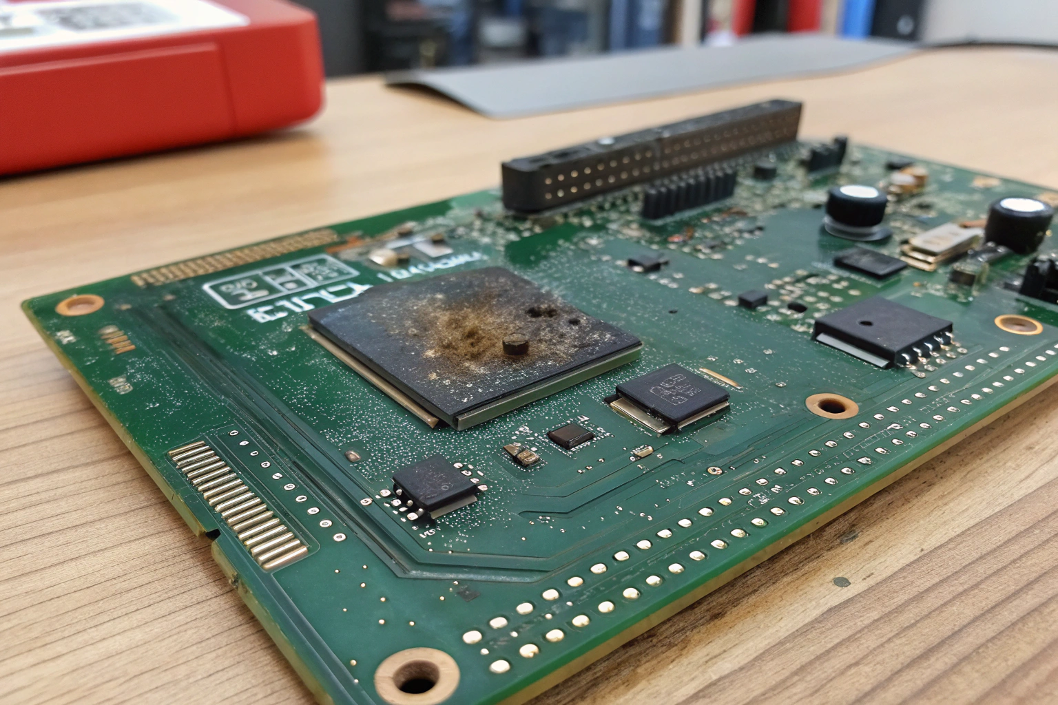
On dense boards, contamination trapped under components or coatings accelerates failure and cannot be removed later.
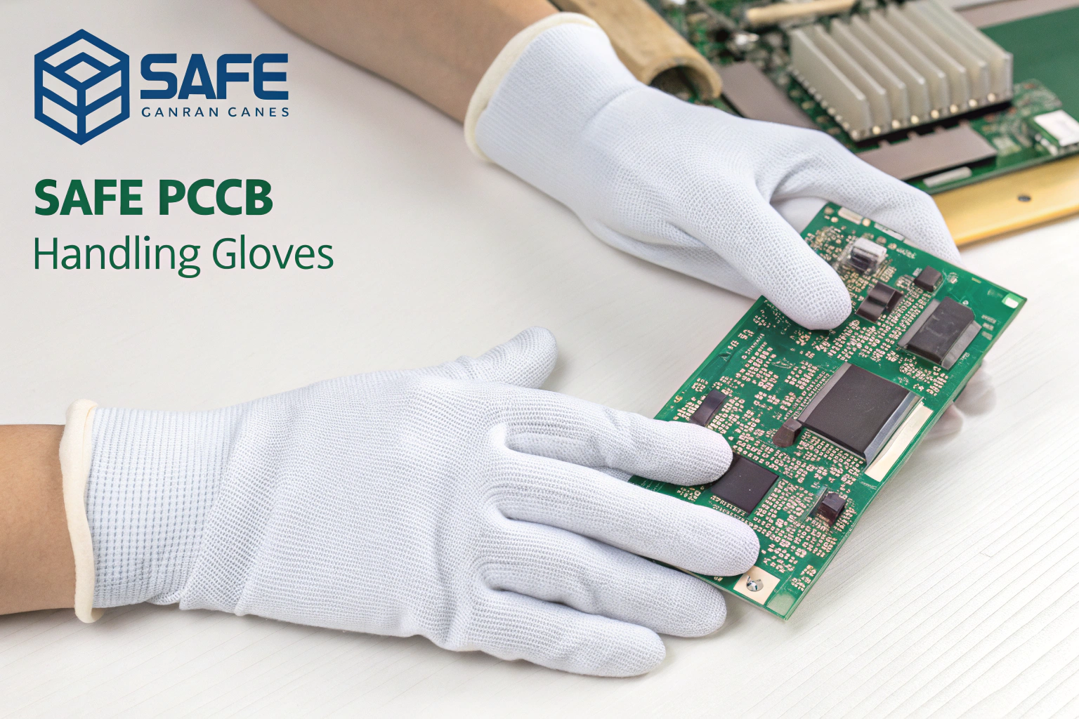
In professional manufacturing, gloves or finger cots are used, and boards are cleaned after soldering. Cleanliness is measured through ionic contamination testing, not assumed.
Mechanical Stress From Handling Can Damage PCBs
PCBs are rigid but fragile.
Improper handling creates hidden defects.
Touching a PCB often involves bending, pressing, or lifting by unsupported edges. This mechanical stress can cause:
- Micro-cracks in solder joints
- Cracked vias in multilayer boards
- Pad lifting near connectors
- Board warping
These defects are often invisible and pass initial testing. Failures appear later during thermal cycling or vibration in real use.
Factory workshops use carriers, pallets, and fixtures to support boards fully and prevent flexing. Operators are trained to handle PCBs only at designated edges.
Factory Workshops Treat PCB Handling as a Process Step
Handling rules are part of quality control.
They are not optional.
In professional PCB and PCBA manufacturing, handling is governed by:
- ESD-protected production lines
- Defined handling points and procedures
- Controlled humidity and temperature
- Anti-static gloves and trays
- Operator training and audits
Boards move through printing, placement, reflow, inspection, testing, and packaging with minimal manual contact. Every unnecessary touch is considered a risk factor.
This discipline ensures consistency across thousands of boards and prevents latent defects caused by casual handling.
When Is It Acceptable to Touch a PCB?
Acceptability depends on control, not intention.
Uncontrolled contact always carries risk.
Touching a PCB may be acceptable only when:
- The board is unpowered
- ESD protection is active
- Gloves or finger cots are used
- Contact is limited to board edges
- Sensitive areas are avoided
Even under these conditions, handling is minimized. The preferred approach is always to avoid direct contact whenever possible.
This philosophy improves yield, reduces field failures, and extends product lifespan.
Conclusion
PCBs are safe to touch for humans, but touching them can damage the PCB through electrostatic discharge, contamination, and mechanical stress. These effects are often invisible at first and appear later as corrosion, intermittent faults, or early failure. In professional manufacturing, PCB handling is treated as a controlled process supported by ESD protection, cleanliness standards, and trained operators. Factory workshops are designed to minimize direct contact and eliminate uncontrolled handling. Reliable electronic products are built not only through good design and soldering, but also through disciplined handling practices that protect the PCB from unnecessary human contact throughout its entire lifecycle.
