
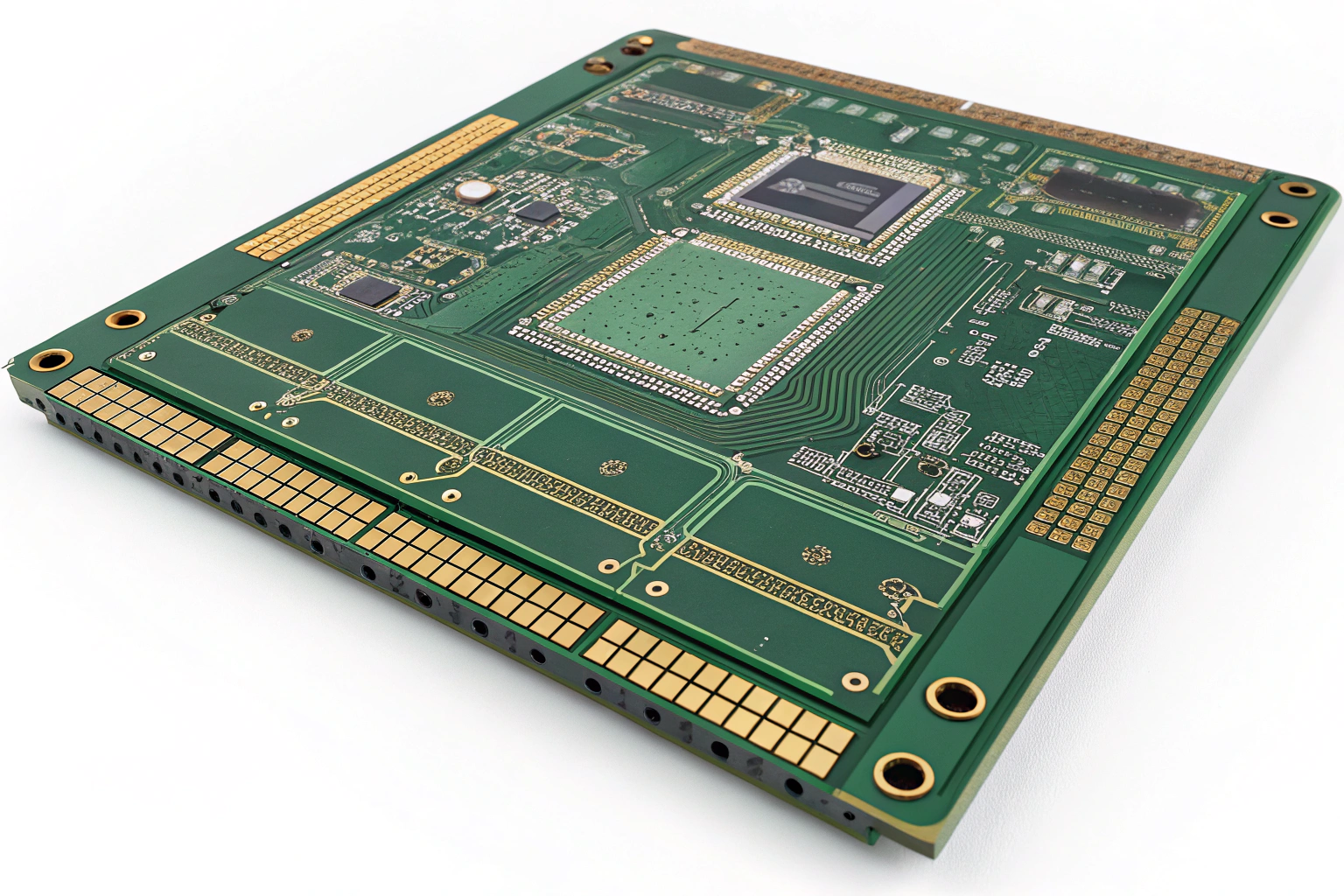
Multilayer printed circuit boards (PCBs) are the foundation of modern electronic products. From industrial control systems to medical equipment and smart devices, multilayer PCBs make it possible to integrate complex circuits into compact and reliable assemblies. Understanding how a multilayer PCB works helps engineers and product teams make better decisions in design, manufacturing, and long-term reliability.

A multilayer PCB works by stacking multiple conductive copper layers separated by insulating materials, then electrically connecting them through vias. This structure allows complex circuits, stable signal transmission, and compact layouts while improving performance, reliability, and noise control in advanced electronic products.
To fully understand multilayer PCBs, it is necessary to look at their internal structure, signal behavior, materials, manufacturing processes, and factory-level quality control. The following sections explain these aspects step by step from a manufacturing and engineering perspective.
What Is the Basic Structure of a Multilayer PCB?
Multilayer PCBs are built by stacking several copper layers with insulation layers in between. Each copper layer carries specific circuit functions such as signal routing, power distribution, or grounding.

The core structure usually includes:
- Signal layers for routing electrical signals
- Power planes for stable voltage distribution
- Ground planes for noise control and signal reference
- Prepreg and core materials for insulation and bonding
Unlike single-layer or double-layer boards, multilayer PCBs allow vertical interconnections between layers using plated vias. These vias form electrical paths that connect circuits across layers, enabling higher wiring density and shorter signal paths.
From a manufacturing viewpoint, layer symmetry and stack-up design are critical. An unbalanced stack-up can lead to warping during lamination and soldering. Proper layer arrangement improves mechanical stability, thermal balance, and signal integrity.
How Do Signals Travel Inside a Multilayer PCB?
Signal transmission inside a multilayer PCB is controlled by copper traces and reference planes. Each signal layer is usually placed adjacent to a ground or power plane to form a controlled impedance environment.
High-speed signals travel as electromagnetic waves rather than simple electrical currents. The return path, usually through the ground plane, is as important as the signal trace itself. A well-designed multilayer PCB ensures that signal and return paths are close and continuous.
Key signal control methods include:
- Controlled impedance traces
- Dedicated ground planes
- Short via transitions
- Reduced loop area
Poor layer planning can cause signal reflection, crosstalk, and electromagnetic interference. Multilayer designs reduce these risks by separating noisy circuits from sensitive signals and by using internal planes as shields.
Why Are Power and Ground Planes So Important?
Power and ground planes are the backbone of a multilayer PCB. They provide stable voltage distribution and reduce noise caused by current fluctuations.
A solid ground plane offers:
- Low impedance return paths
- Reduced electromagnetic interference
- Improved signal stability
Power planes help distribute current evenly and support decoupling capacitors placed close to components. In multilayer boards, separating power and ground layers reduces voltage drop and heat concentration.
From a manufacturing perspective, plane integrity must be protected during etching and drilling. Breaks or voids in planes can cause unstable performance that is difficult to detect after assembly. Proper design rules and inspection processes are essential.
How Are Multilayer PCBs Manufactured in the Factory?
Multilayer PCB manufacturing is a precise and tightly controlled process. It starts with inner layer fabrication, where copper patterns are etched onto core materials. These inner layers are then inspected before lamination.

Main manufacturing steps include:
- Inner layer imaging and etching
- Layer alignment and stacking
- Lamination under heat and pressure
- Drilling of vias and holes
- Copper plating and via filling
- Outer layer patterning
- Surface finish application
In the factory workshop, lamination is one of the most critical stages. Temperature, pressure, and time must be precisely controlled to ensure strong bonding without damaging inner circuits. Automated optical inspection is often applied before and after lamination to prevent hidden defects.
What Materials Are Used in Multilayer PCBs?
Material selection directly affects performance, durability, and manufacturing yield. Most multilayer PCBs use FR4 epoxy glass laminate due to its balance of cost, strength, and electrical performance.
For demanding applications, other materials may be used:
- High-Tg FR4 for thermal stability
- Rogers materials for high-frequency designs
- Low-loss laminates for signal integrity
Prepreg materials act as bonding layers during lamination. Their resin flow characteristics determine how well layers bond and how void-free the final board will be. Material compatibility across layers is carefully verified during engineering review to avoid delamination and reliability issues.
How Does PCBA Assembly Affect Multilayer PCB Performance?
After PCB fabrication, assembly plays a major role in overall performance. Multilayer boards often carry fine-pitch components, BGA packages, and dense layouts that require precise SMT processes.
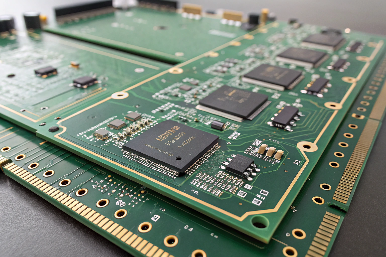
Key assembly considerations include:
- Accurate solder paste printing
- Controlled reflow profiles
- Reliable via-in-pad processing
- Thermal balance across layers
Factory workshops use AOI, X-ray inspection, and functional testing to verify solder joints and internal connections. Multilayer boards store more heat, so reflow temperature curves must be carefully optimized to avoid solder defects or inner layer stress.
Conclusion
From a manufacturing perspective, the performance of a multilayer PCB is not determined by design alone. Inner layer accuracy, lamination pressure control, drilling precision, copper plating quality, and surface finish consistency all play decisive roles in final reliability. Even small deviations in materials or process parameters can lead to hidden defects such as delamination, impedance mismatch, or long-term thermal stress. For this reason, strict process control, standardized inspection methods, and experienced engineering oversight are essential throughout production.
As electronic products continue to evolve toward higher speed, smaller size, and greater functional integration, multilayer PCB technology will remain indispensable. Boards designed and manufactured with proper stack-up planning, material selection, and assembly discipline deliver stable performance not only at the prototype stage but also across long production cycles. A well-executed multilayer PCB is therefore not just a circuit carrier, but a critical foundation that supports product reliability, electrical performance, and long-term application success.
