
Knowing how many layers a PCB has is essential for understanding its electrical capability, signal integrity, cost structure, and manufacturing complexity. PCB layer count affects routing density, impedance control, heat dissipation, and overall reliability, making it a key factor in both design evaluation and production planning.
The number of PCB layers can be identified by visual inspection, documentation review, cross-section analysis, and manufacturing process indicators.
Each method provides different levels of accuracy and is commonly used at different stages of development and production.
Understanding these identification methods helps avoid design misjudgment, quotation errors, and production risks. The following sections explain the most reliable ways to determine PCB layer count, combined with real manufacturing and workshop practices.
Can PCB Layers Be Identified by Visual Inspection?
Surface observation provides limited but useful clues.
Visual inspection is often the first step to estimate PCB layer count, especially for simple boards.
Single-layer PCBs usually have copper traces on only one side, while double-layer PCBs show visible copper patterns and vias on both sides. Through-hole vias connecting top and bottom layers are easy to identify under normal lighting.
However, once a PCB exceeds two layers, visual inspection becomes unreliable. Inner copper layers are fully embedded within the laminate and cannot be seen from the outside. Blind vias, buried vias, and via-in-pad designs further reduce visibility.
In production workshops, visual checks are mainly used for quick classification during incoming inspection. Final confirmation always relies on documentation or physical analysis.
How Does PCB Documentation Show Layer Count?
Design files provide the most direct answer.
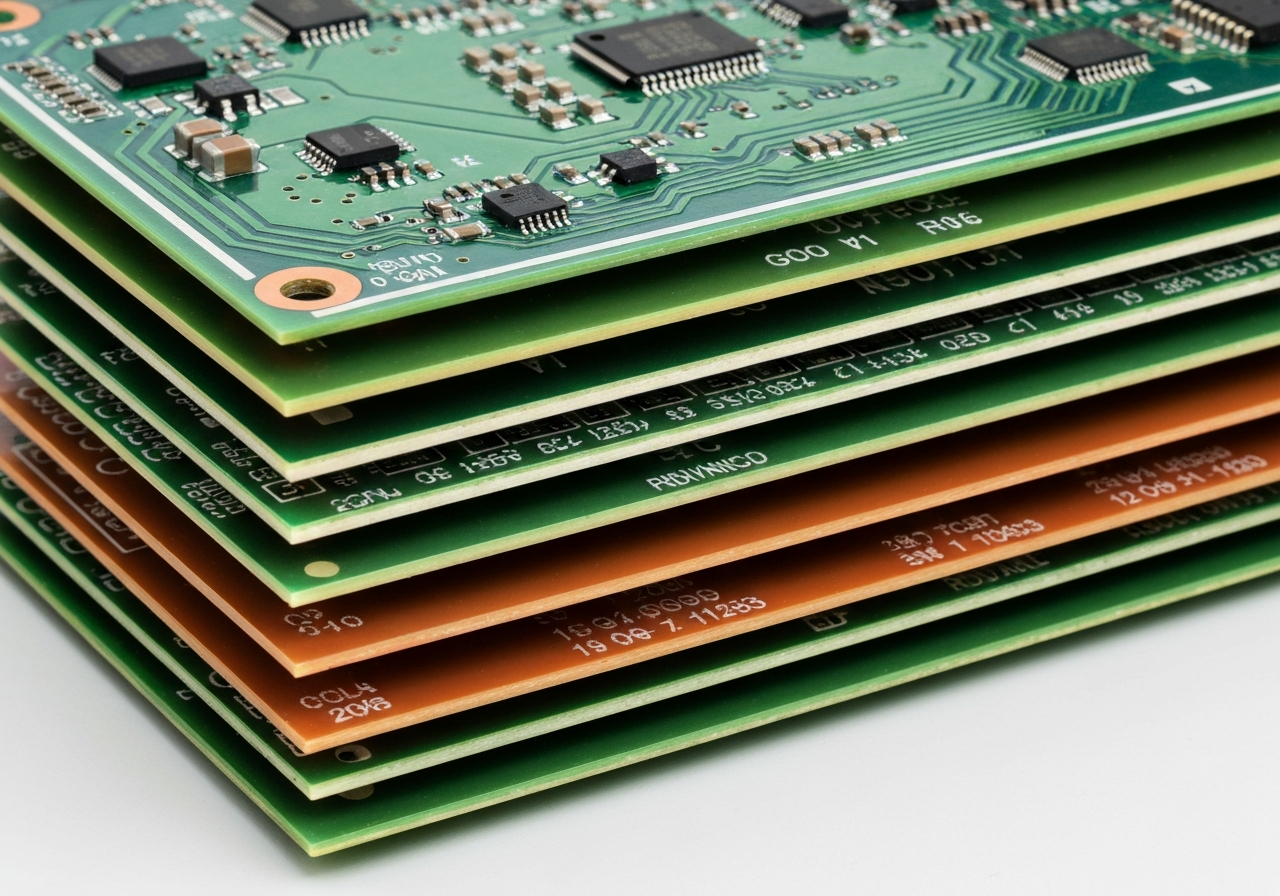
PCB layer count is clearly defined in design documents such as Gerber files, stack-up drawings, and fabrication notes.
A stack-up drawing shows each copper layer, prepreg, and core material in sequence. Gerber files usually include separate files for top copper, bottom copper, and each internal layer, often named as Inner Layer 1, Inner Layer 2, and so on.
From a manufacturing standpoint, documentation review is the standard method used before quoting and production. It determines lamination cycles, material selection, drilling complexity, and inspection requirements.
Missing or unclear layer information often leads to delays, engineering questions, or incorrect cost estimation. This is why complete and accurate stack-up data is considered mandatory before production release.
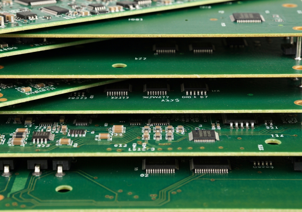
Can Vias Indicate the Number of PCB Layers?
Vias offer indirect but valuable information.
The type and structure of vias used on a PCB can suggest whether the board is multilayer.
Through-hole vias typically connect all layers from top to bottom, which is common in multilayer boards. Blind vias connect an outer layer to an inner layer, while buried vias connect inner layers only.
The presence of blind or buried vias almost always indicates a four-layer or higher PCB. These via types require additional drilling and lamination steps, increasing process complexity.
In SMT workshops, via structures affect stencil design, solder paste behavior, and inspection difficulty. Identifying via types early helps engineers assess manufacturing risk and testing strategy.
How Does Cross-Section Analysis Reveal PCB Layers?
Physical analysis provides absolute confirmation.
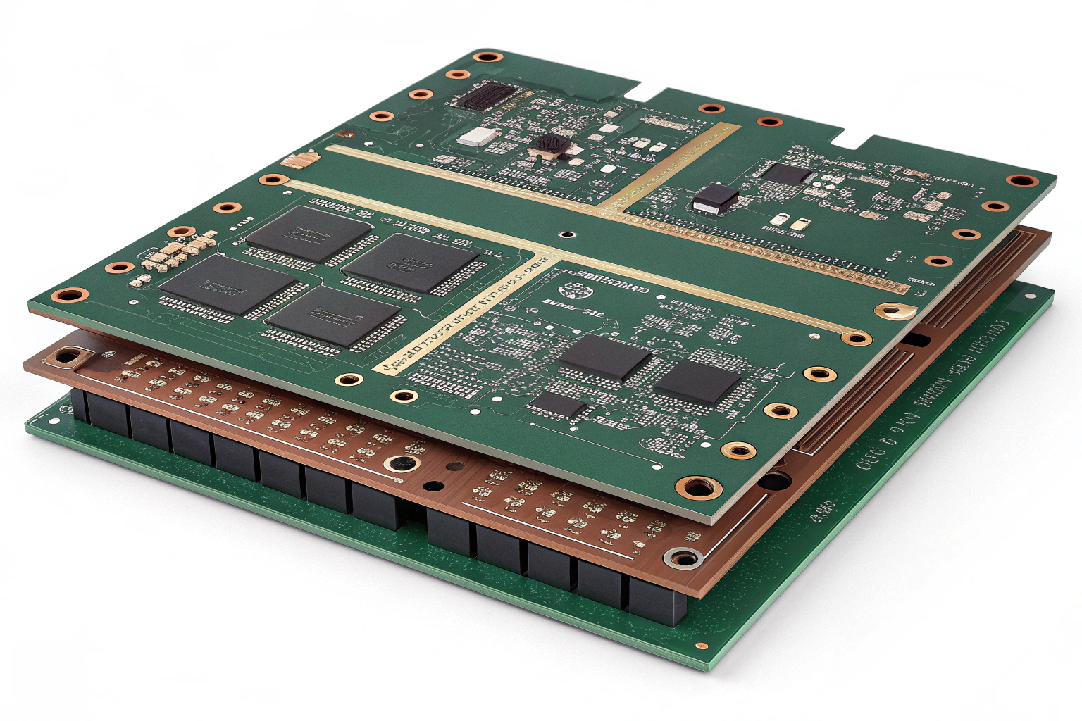
Cross-section analysis involves cutting a PCB sample and examining it under a microscope to directly count copper layers.
This method clearly shows copper thickness, dielectric spacing, and layer sequence. It is commonly used for failure analysis, process validation, and quality audits.
In manufacturing environments, cross-section analysis is not used for every board due to cost and time. Instead, it is applied selectively for new products, high-reliability applications, or when defects such as delamination or via cracking are suspected.
Cross-section results are often compared against stack-up drawings to verify that production matches design intent.
Does PCB Thickness Help Determine Layer Count?
Thickness gives hints, not final answers.
PCB thickness can suggest possible layer count but cannot confirm it alone.
Standard thickness values such as 1.6 mm are used across different layer counts. A four-layer board and a six-layer board can share the same overall thickness while using thinner cores and prepregs.
However, unusually thick boards may indicate higher layer counts or heavy copper designs. Thickness data is useful when combined with documentation and via analysis.
In production planning, thickness affects reflow profiles, panel rigidity, and depaneling methods, making it an important parameter beyond layer identification.
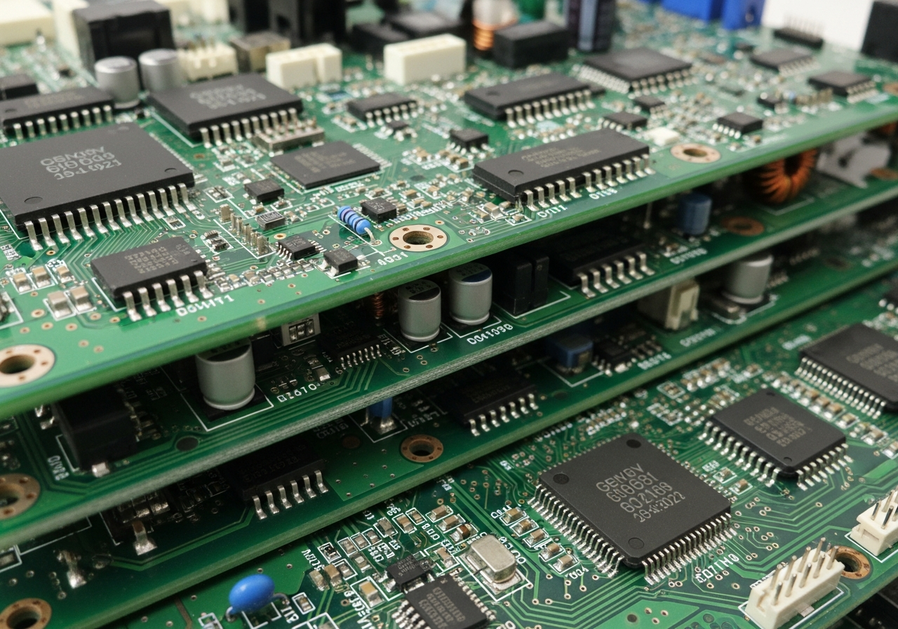
How Do Manufacturing Processes Reflect PCB Layer Count?
Layer count directly impacts factory workflow.

The number of PCB layers determines lamination cycles, drilling operations, inspection steps, and production lead time.
Single and double-layer boards require no lamination, while multilayer boards need precise stacking and bonding under heat and pressure. More layers mean tighter alignment tolerance and higher risk of defects such as misregistration or delamination.
In SMT workshops, multilayer PCBs often support higher component density and complex routing. This influences placement accuracy, thermal balance during reflow, and testing coverage.
Manufacturing engineers rely on layer count information to plan materials, equipment usage, and quality checkpoints, ensuring consistency from prototype builds to volume production.
Conclusion
Determining how many layers a PCB has requires more than surface observation. Visual inspection, design documentation, via structure analysis, cross-section testing, thickness reference, and manufacturing process indicators all contribute to accurate identification. Among these methods, documentation and stack-up drawings remain the most reliable, while physical analysis provides final confirmation when needed. Understanding PCB layer count is essential for correct manufacturing planning, quality control, and long-term product reliability.
