
PCB thickness is one of the most standardized parameters in electronics manufacturing. Among all available options, 1.6 mm has become the most widely used default thickness for rigid PCBs across many industries. This value is not arbitrary; it is the result of long-term material evolution, process optimization, and manufacturing practicality.
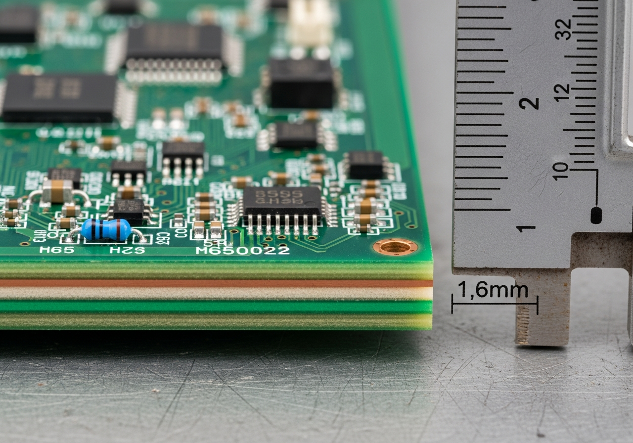
PCBs are commonly 1.6 mm thick because this thickness provides an optimal balance between mechanical strength, electrical performance, assembly stability, component compatibility, and factory process reliability.
It fits well within mature manufacturing process windows and supports consistent quality at scale.
The reasons behind this standard become clear when examined from historical, mechanical, assembly, and factory process perspectives.
Historical and Material Origins of the 1.6 mm Standard
Standards often originate from material availability.
The 1.6 mm PCB thickness traces back to early laminate materials based on 1/16 inch (≈1.57 mm) cores. As the electronics industry standardized around FR-4 materials, this thickness proved practical and was gradually normalized to 1.6 mm.
Once adopted, PCB fabrication equipment, tooling, drilling parameters, and inspection systems were all optimized around this thickness. Over time, it became the default reference used in design rules, component datasheets, and manufacturing documentation.
This historical consistency laid the foundation for today’s highly stable 1.6 mm production ecosystem.
Mechanical Strength and Structural Stability
Mechanical rigidity is a primary factor.
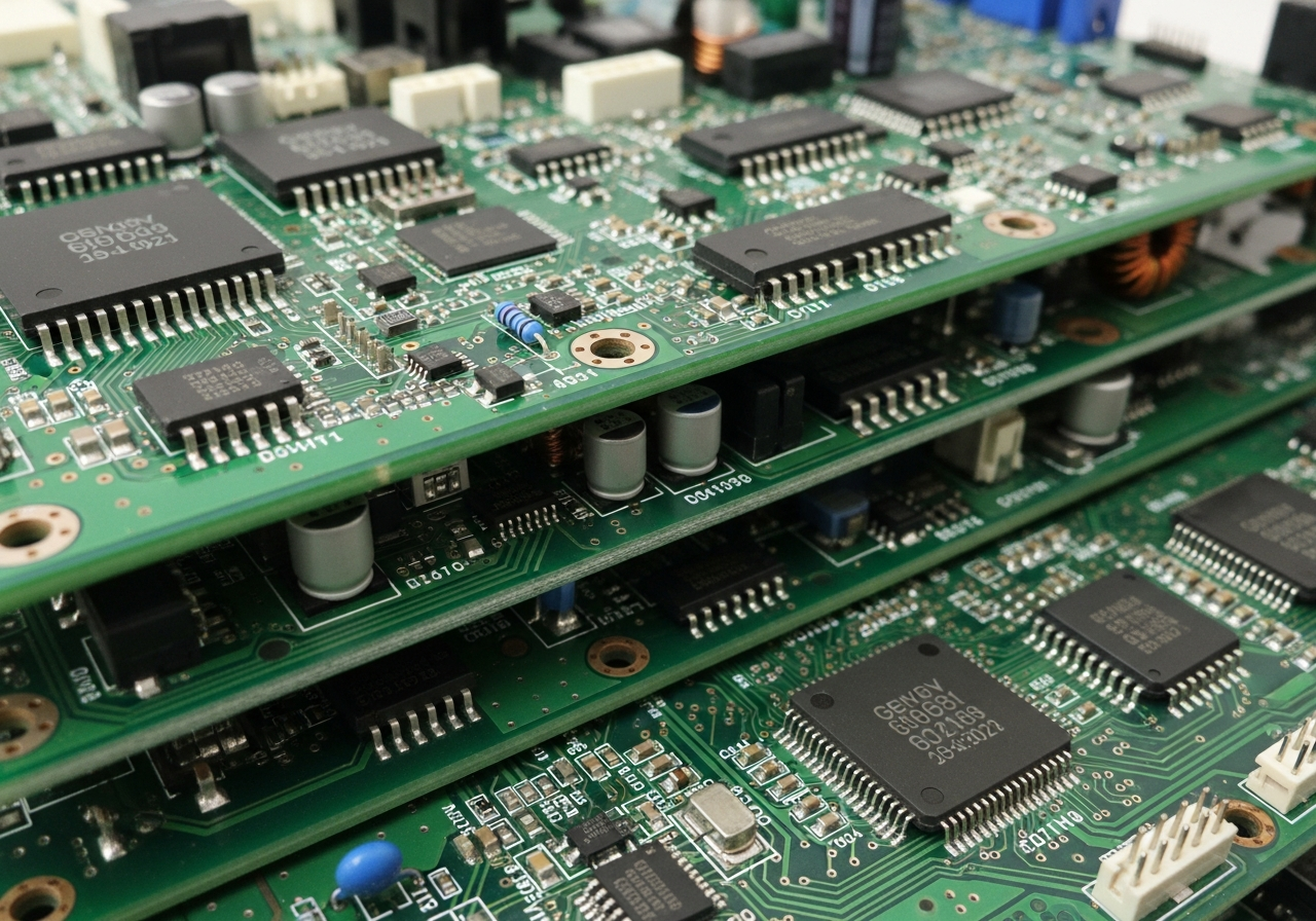
A 1.6 mm PCB offers sufficient stiffness to resist bending during handling, assembly, installation, and long-term operation.
Boards thinner than 1.2 mm are more prone to flexing, which can stress solder joints and vias. Thicker boards increase weight and cost without proportional benefit for most applications.
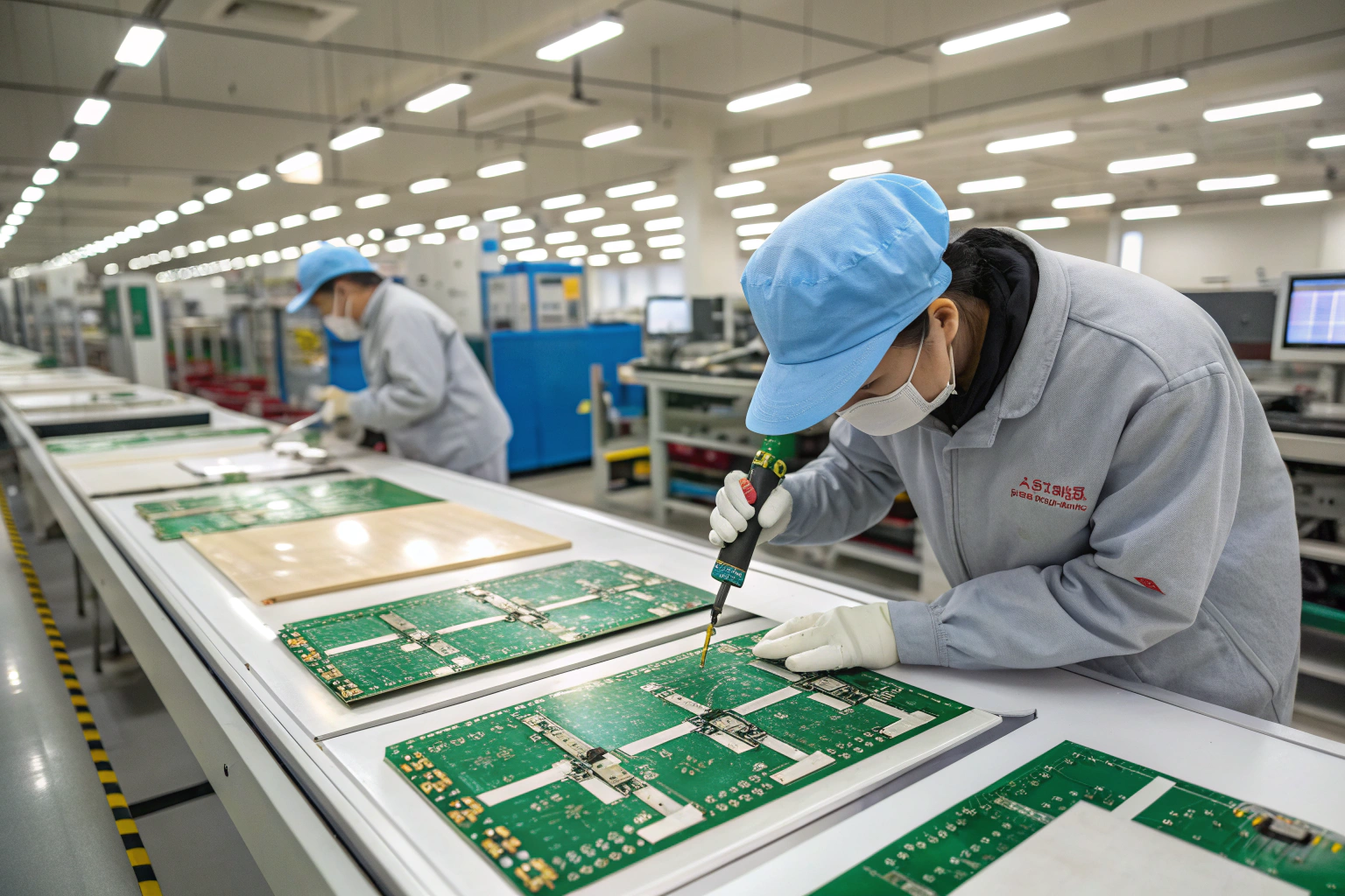
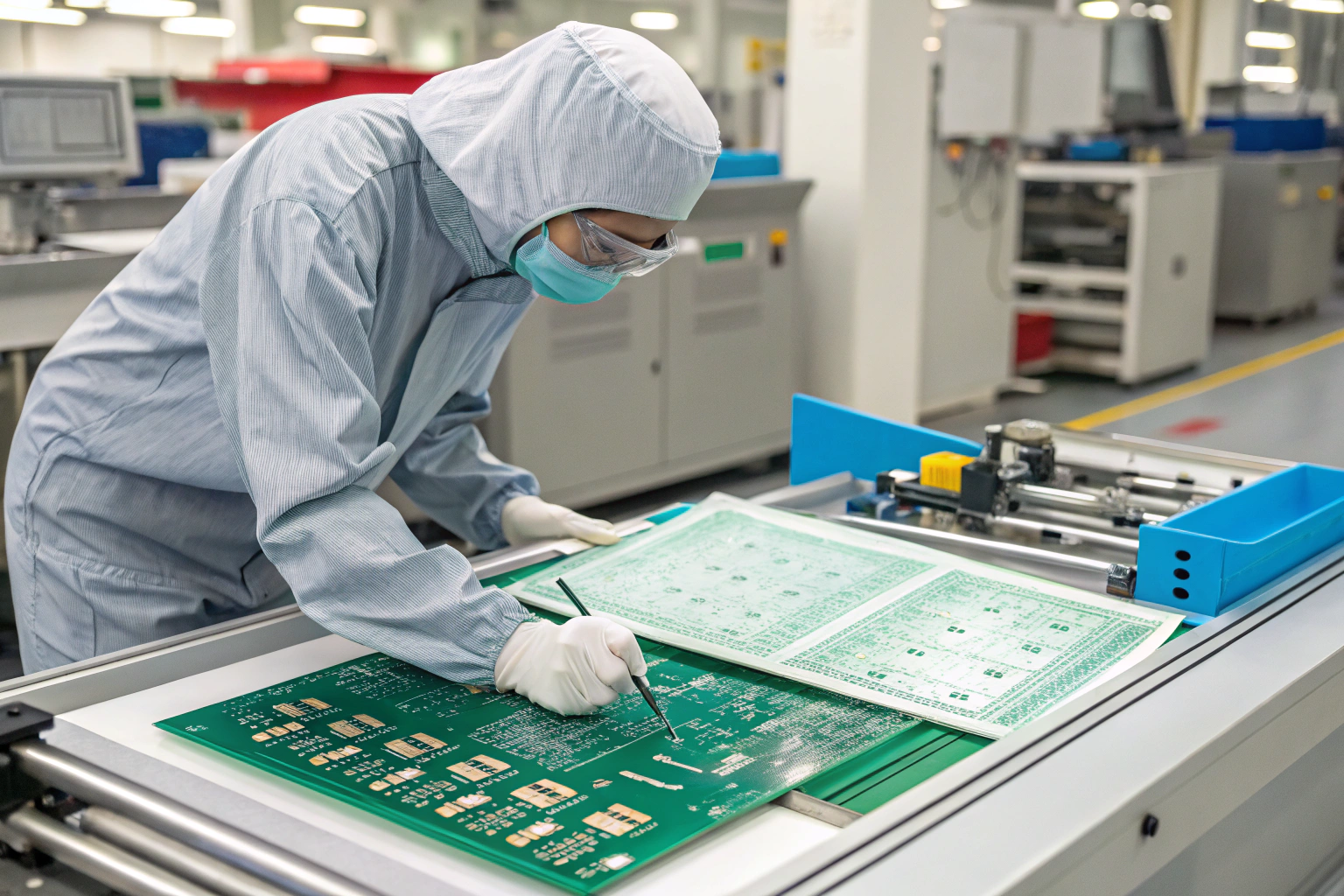
In factory workshops, 1.6 mm boards maintain flatness during transport through SMT lines, manual handling, and fixture loading. This stability reduces the risk of mechanical defects and improves assembly consistency.
Compatibility With SMT Assembly Processes
Assembly equipment favors predictable thickness.
During SMT assembly, PCB thickness affects conveyor support, edge clamping, thermal behavior, and coplanarity during reflow soldering.
A 1.6 mm board provides balanced thermal mass, allowing it to heat and cool evenly during reflow. Thinner boards are more sensitive to thermal gradients and warpage, while thicker boards require longer heating cycles.
Most SMT lines, reflow ovens, and support systems are calibrated around 1.6 mm boards. Using this thickness minimizes setup adjustments and improves line efficiency in high-mix or volume production.
Component and Connector Compatibility
Many components assume a 1.6 mm board.
Through-hole components, connectors, card-edge interfaces, and mechanical fasteners are often designed with 1.6 mm PCB thickness as a reference.
Pin length, retention force, and mating depth frequently depend on this thickness. Deviating from 1.6 mm may require custom components or mechanical redesign, increasing complexity and risk.
From a production standpoint, standard thickness simplifies sourcing, assembly validation, and mechanical fit verification.
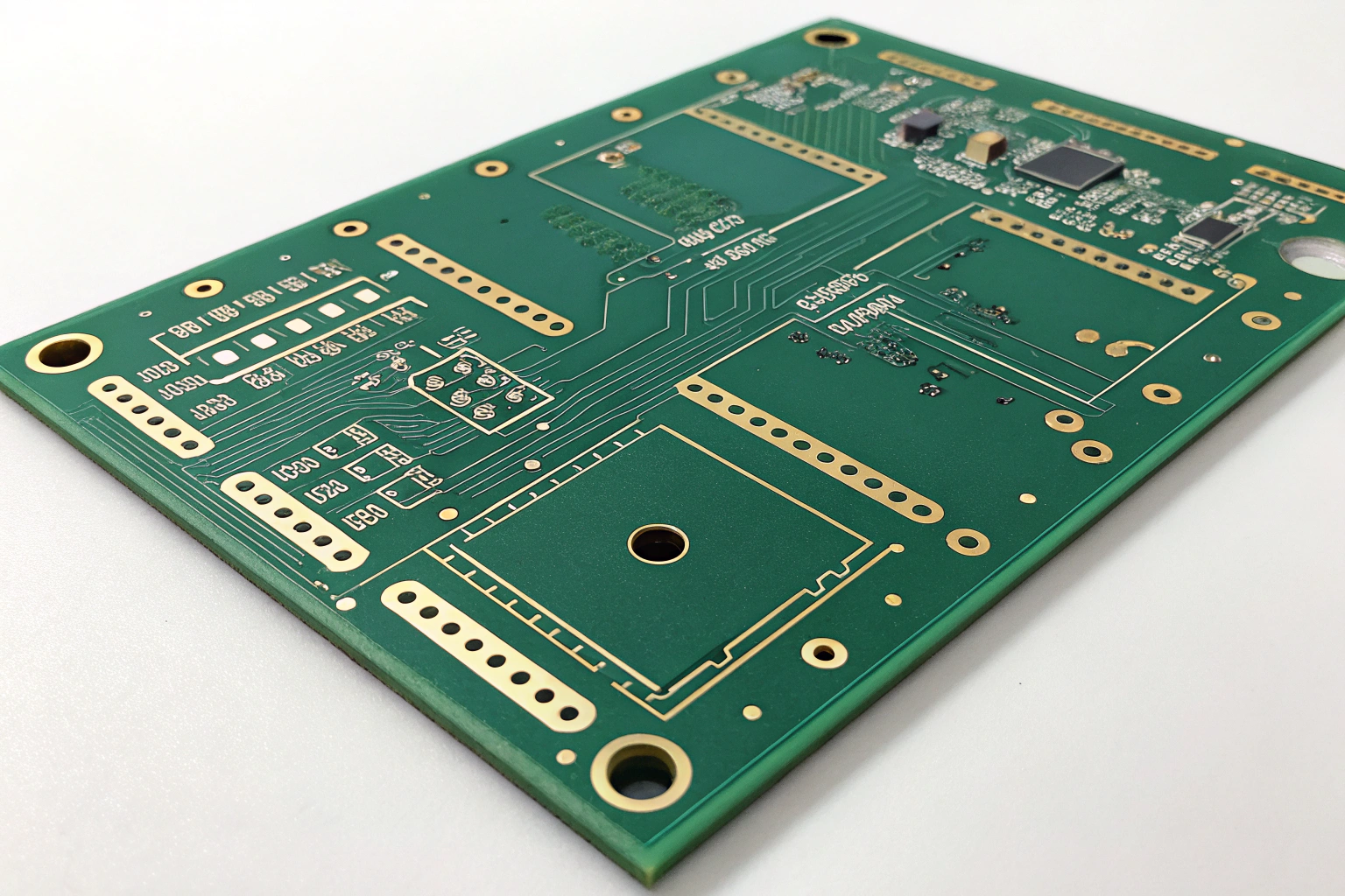
Manufacturing Efficiency and Process Stability
Factory processes are optimized for 1.6 mm.
PCB factories stock core and prepreg combinations specifically designed to produce 1.6 mm boards with high yield.
Key advantages in production include:
- Stable lamination thickness control
- Predictable drilling aspect ratios
- Consistent copper plating quality
- Reduced warpage and delamination risk
Because the process window is wide and well understood, defect rates are lower and rework is minimized. This makes 1.6 mm boards ideal for both prototype builds and volume manufacturing.
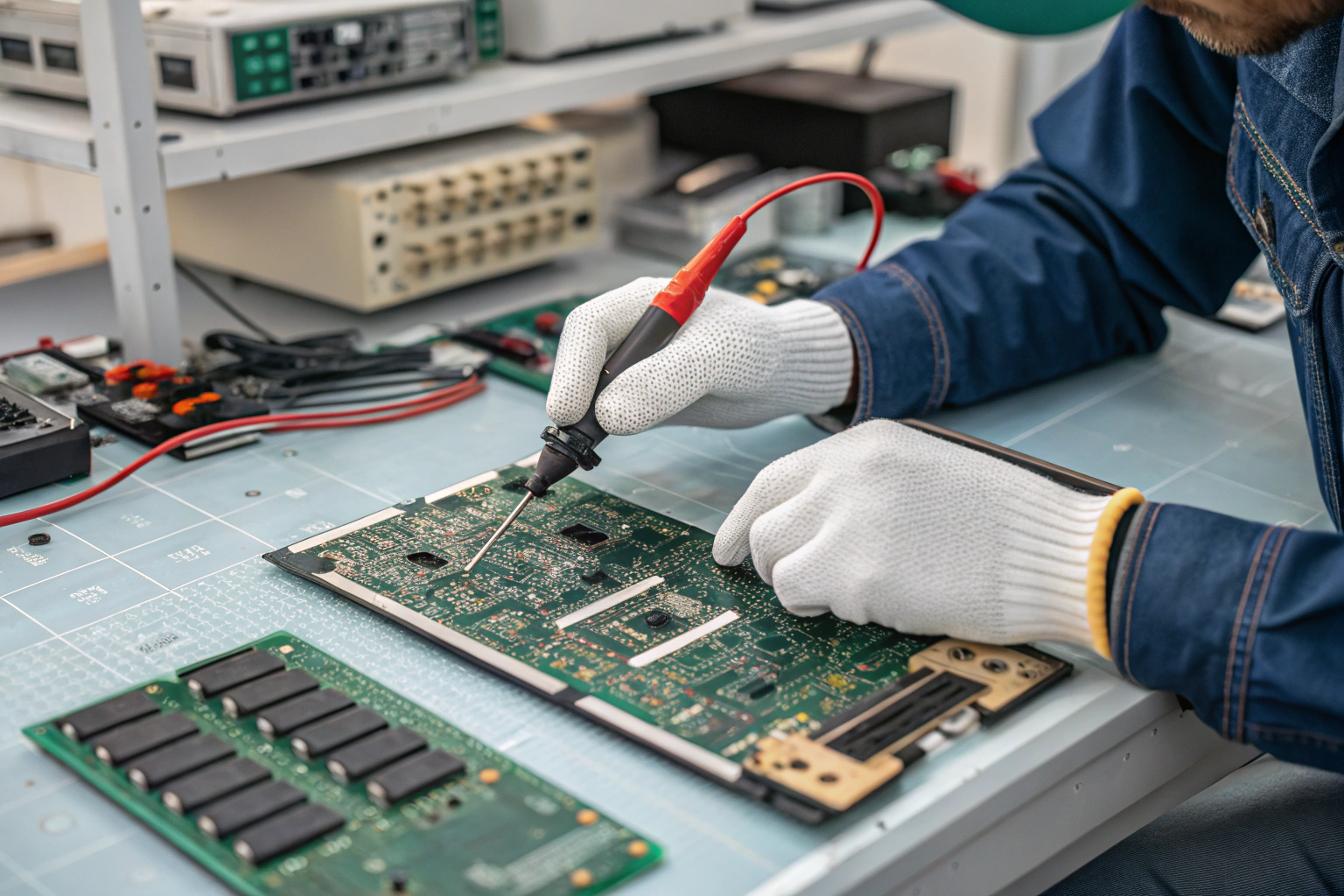
Impact on Testing, Fixtures, and Quality Control
Consistency simplifies testing.
Electrical test fixtures, probe travel depth, and support pin layouts are commonly designed around 1.6 mm PCB thickness.
Boards thinner than standard may flex under probe pressure, causing false failures. Thicker boards may prevent proper contact. Using 1.6 mm ensures repeatable test results and reliable inspection data.
From a quality control perspective, standardized thickness improves traceability, inspection accuracy, and long-term consistency across production batches.
When Other Thicknesses Are Used
Standard does not mean universal.
While 1.6 mm is the default, other thicknesses are used when justified by product requirements:
- Thinner boards (0.8–1.2 mm) for compact or weight-sensitive designs
- Thicker boards (2.0 mm or more) for high-power or mechanically demanding applications
However, these alternatives usually involve tighter process control, higher cost, or additional engineering validation. When no strong constraint exists, 1.6 mm remains the safest and most economical choice.
Conclusion
PCBs are commonly 1.6 mm thick because this dimension represents a proven balance between mechanical strength, assembly stability, electrical reliability, component compatibility, and manufacturing efficiency. It is deeply rooted in material standards and supported by decades of factory process optimization.
From the factory floor to final inspection, 1.6 mm PCBs move through production with predictable behavior, stable yield, and consistent quality. While other thicknesses serve specific needs, 1.6 mm continues to be the industry benchmark because it reduces risk, simplifies manufacturing control, and delivers dependable performance across a wide range of electronic products.
