
A 1 layer PCB is the most basic form of printed circuit board and is widely used in simple electronic products where circuit complexity, signal speed, and component density are low. Despite its simplicity, it remains an important solution in electronics manufacturing due to its cost efficiency and ease of production.
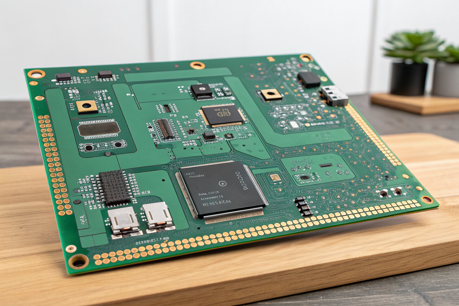
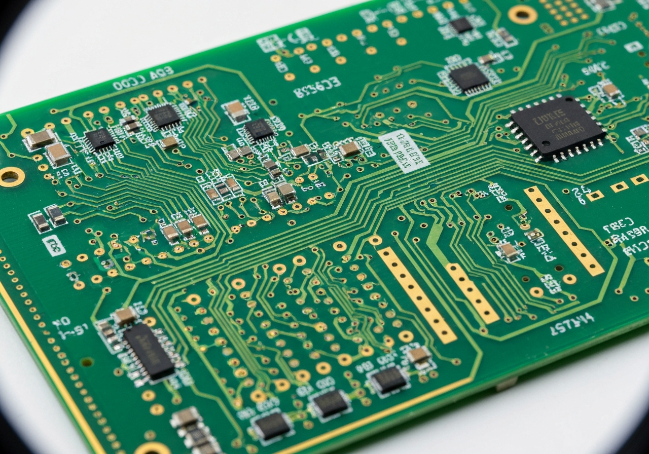
A 1 layer PCB is a circuit board that has copper traces on only one side of the insulating substrate, with no internal or opposite-side copper layers.
All electrical connections are routed on a single copper layer.
Understanding the structure, applications, and manufacturing characteristics of 1 layer PCBs helps clarify when this type of board is suitable and when more complex multilayer designs are required.
How Is a 1 Layer PCB Structured?
The structure is simple and easy to identify.
A typical 1 layer PCB consists of:
- One copper layer for signal and power routing
- One insulating substrate, usually FR-4 or phenolic paper
- Optional solder mask on the copper side
- Silkscreen for component marking
All components are mounted on one side of the board, and there are no plated through-holes connecting multiple copper layers. Any required crossovers must be handled using jumper wires or zero-ohm resistors.
From a fabrication perspective, this structure eliminates lamination steps, making production faster and more straightforward compared to multilayer boards.
What Are the Typical Applications of a 1 Layer PCB?
Simple functions favor simple boards.
1 layer PCBs are commonly used in products such as:
- Power adapters and chargers
- LED lighting modules
- Simple control boards
- Consumer appliances with basic logic
- Educational and training electronics
These applications usually involve low-speed signals, limited component count, and relaxed EMI requirements. For such use cases, a single copper layer is sufficient to meet electrical and mechanical needs.
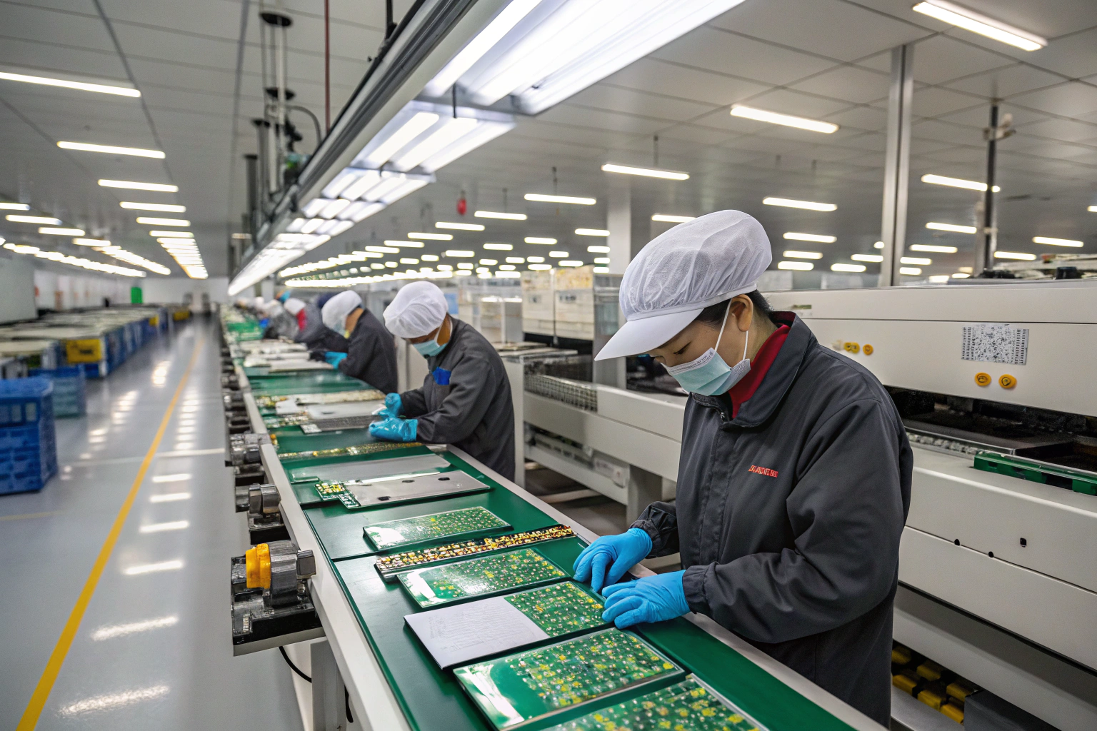
In manufacturing, these boards are often produced in large volumes with highly standardized processes, which helps maintain stable quality and low unit cost.
What Are the Advantages of a 1 Layer PCB?
Simplicity brings clear benefits.

The main advantages include:
- Lower fabrication cost
- Shorter production lead time
- Easier inspection and repair
- Higher yield due to fewer process steps
Without inner layers or complex via structures, defect risks such as delamination or inner-layer misregistration are eliminated. Electrical testing is also simpler, as all traces are accessible from one side.
In factory workshops, these boards move quickly through etching, drilling (if required), solder mask, and surface finish processes, making them suitable for cost-sensitive products.
What Are the Limitations of a 1 Layer PCB?
Design flexibility is limited.
Because routing is restricted to one copper layer, 1 layer PCBs face several constraints:
- Limited routing density
- Larger board size for complex circuits
- Increased use of jumpers or wire links
- Poorer signal integrity for high-speed designs
Power and ground routing must share the same layer as signal traces, which can increase noise and reduce electrical performance. These limitations become critical in designs involving microcontrollers, RF signals, or dense component layouts.
As a result, many designs transition to double-layer or multilayer PCBs once functional requirements increase.
How Is a 1 Layer PCB Manufactured?
The process is direct and well controlled.

Typical manufacturing steps include:
- Base material cutting
- Copper pattern imaging and etching
- Drilling for through-hole components
- Solder mask application (optional)
- Surface finish processing
- Silkscreen printing
Because no lamination is required, process variability is low. In production workshops, this results in stable yields and predictable quality. Assembly is usually done using DIP or mixed technology, although SMT is also possible on single-layer boards.
How Does a 1 Layer PCB Perform in Assembly and Testing?
Assembly and testing are straightforward.
During assembly, components are placed on one side, simplifying placement programming and reducing alignment risks. Thermal behavior during wave soldering or reflow is easy to control due to the uniform copper distribution.
Testing access is excellent because all nets are exposed. This allows simple test fixtures and fast functional testing. Repair and rework are also easier compared to multilayer designs.
However, as component density increases, assembly efficiency drops due to routing limitations, making higher-layer boards more practical.
Conclusion
A 1 layer PCB is a single-sided circuit board with all copper traces located on one surface of the substrate. Its simple structure makes it cost-effective, easy to manufacture, and reliable for low-complexity electronic products. While it offers clear advantages in simplicity and production efficiency, its routing and performance limitations restrict its use in advanced designs. For basic control, power, and lighting applications, the 1 layer PCB remains a practical and widely used solution in modern electronics manufacturing.
