
A 4 layer PCB represents one of the most widely adopted multilayer board structures in modern electronics manufacturing. It marks the transition from basic circuit routing to a more controlled and reliable electrical architecture, where signal quality, power stability, and manufacturability become core design objectives.
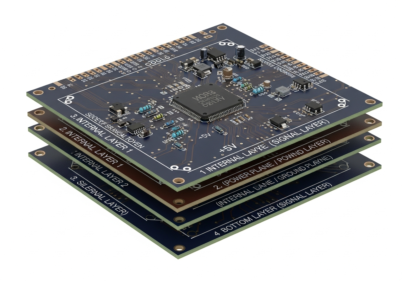
A 4 layer PCB is a printed circuit board that contains four copper layers laminated into one structure, typically arranged as two outer signal layers and two internal layers used for power, ground, or additional signal routing.
This structure significantly improves electrical performance and production stability compared to single or double layer boards.
The sections below explain what a 4 layer PCB means from structural, electrical, and manufacturing perspectives.
What Are the Four Layers in a 4 Layer PCB?
Each layer has a defined functional role.
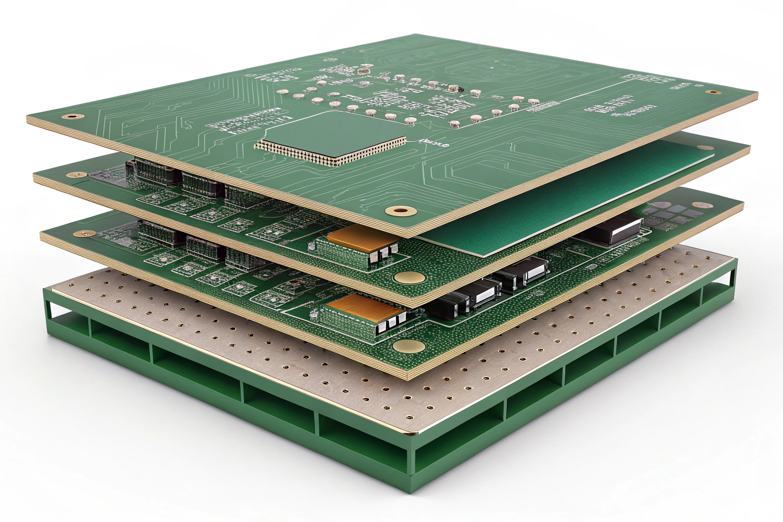
A standard 4 layer PCB stack-up usually includes:
- Top layer: component pads and signal routing
- Inner layer 1: continuous ground plane
- Inner layer 2: power plane or controlled signal layer
- Bottom layer: signal routing and component pads
This arrangement separates signals from power distribution, reducing electrical interference and improving signal reference quality. From a manufacturing standpoint, this symmetric structure also helps maintain mechanical balance during lamination and thermal processing.
How Is a 4 Layer PCB Different from a 2 Layer PCB?
The difference goes beyond copper count.
A 2 layer PCB places all signals, power, and ground on the top and bottom layers. As circuit complexity increases, routing congestion, noise, and power instability become common issues.
A 4 layer PCB introduces internal planes that:
- Provide stable ground reference
- Enable low-impedance power distribution
- Shorten signal return paths
- Reduce routing congestion on outer layers
In production environments, this results in more consistent electrical behavior and fewer functional test variations.
Why Are Power and Ground Planes So Important in a 4 Layer PCB?
Planes stabilize the entire circuit system.
Dedicated power and ground planes distribute current evenly across the board instead of forcing it through narrow traces.
These planes:
- Reduce voltage drop
- Improve decoupling capacitor efficiency
- Minimize electrical noise
- Lower EMI risk
During factory testing and aging processes, boards with solid planes show more stable operation under dynamic load conditions, especially in processor-based and control circuits.
How Does a 4 Layer PCB Improve Signal Integrity?
Signal behavior becomes more predictable.
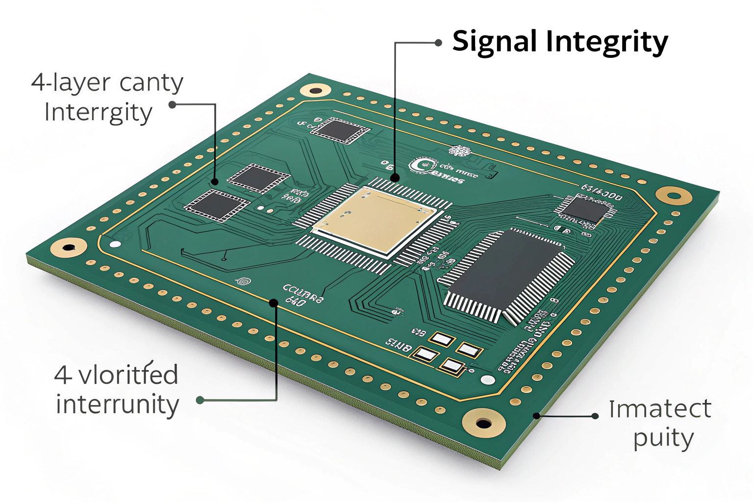
High-speed and sensitive signals benefit from being routed close to a solid ground plane.
In a 4 layer PCB:
- Impedance can be controlled more accurately
- Crosstalk between signals is reduced
- Signal return paths are shorter and clearer
This structure reduces timing variation and signal distortion, making functional performance more consistent across production batches.
How Is a 4 Layer PCB Manufactured?
Manufacturing involves controlled lamination.
Unlike simpler boards, a 4 layer PCB requires inner layer fabrication and lamination before outer layer processing.
Typical manufacturing flow includes:
- Inner layer imaging and etching
- Inner layer AOI inspection
- Stack-up with prepreg and copper foils
- Lamination under controlled heat and pressure
- Drilling, desmear, and copper plating
- Outer layer imaging, solder mask, and surface finish
Because this process is highly standardized, 4 layer PCBs fall within a mature and stable manufacturing window.
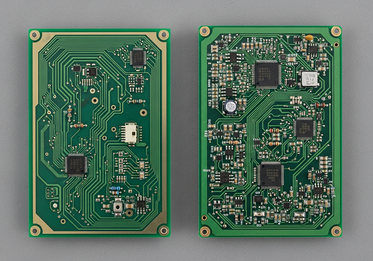
How Does a 4 Layer PCB Perform in Assembly and the Factory Workshop?
Balanced structures assemble more reliably.

The symmetric stack-up of a 4 layer PCB reduces internal stress and board warpage.
In SMT workshops, this leads to:
- Better flatness during reflow soldering
- Improved solder joint consistency
- Higher placement accuracy for fine-pitch components
- More reliable AOI and functional testing results
From a production control perspective, 4 layer boards show higher yield and more predictable assembly behavior compared to complex 2 layer designs.
Conclusion
A 4 layer PCB means more than simply adding extra copper layers. It represents a structured approach to circuit design and manufacturing, where electrical performance, mechanical balance, and production stability are addressed together. By separating signals, power, and ground into dedicated layers, a 4 layer PCB achieves cleaner routing, stronger noise control, and more reliable operation.
From a manufacturing standpoint, 4 layer PCBs benefit from standardized stack-ups, mature lamination processes, and well-established inspection methods. This makes them easier to control in mass production while delivering consistent quality and long-term reliability. As product requirements increase in complexity and performance, the 4 layer PCB remains one of the most practical and widely adopted solutions in modern electronics manufacturing.
