
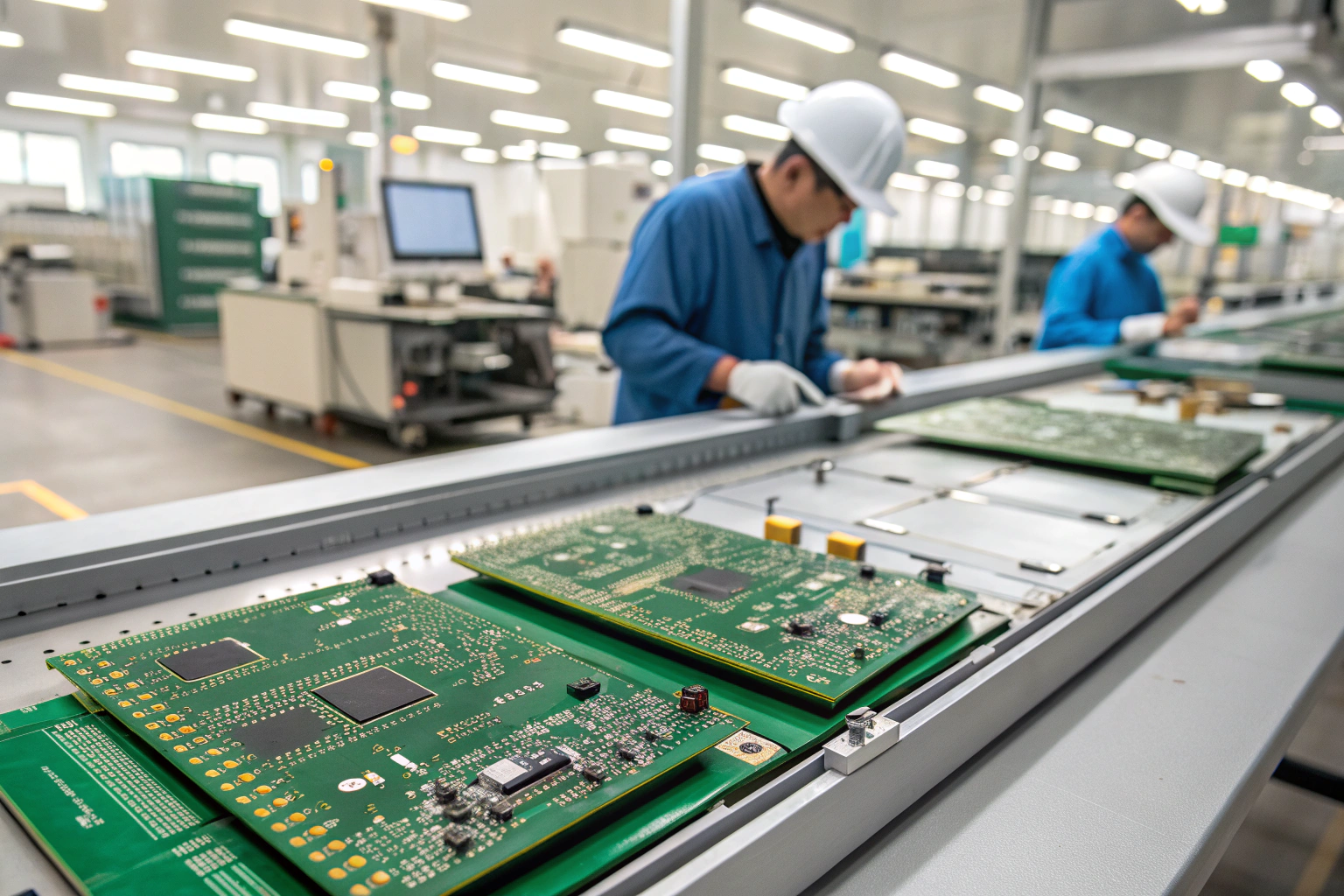
Multilayer PCB manufacturing is a highly controlled industrial process designed to transform multiple independent copper layers into a single, reliable circuit board. Compared with single or double layer boards, multilayer PCBs require stricter material selection, tighter process control, and more inspection steps to ensure electrical and mechanical stability.
A multilayer PCB is manufactured by forming inner circuit layers first, stacking them with prepreg and core materials, laminating them under heat and pressure, then completing drilling, plating, outer-layer processing, testing, and final inspection.
Each stage builds on the previous one and directly affects yield and long-term reliability.
The following sections explain the standard multilayer PCB manufacturing flow from a factory and workshop perspective.
Inner Layer Circuit Fabrication
Inner layers define the electrical foundation.
Manufacturing begins with copper-clad core materials. Each inner layer circuit is created using imaging and etching processes that transfer design data onto copper.
The process typically includes:
- Copper surface cleaning
- Dry film photoresist lamination
- UV exposure with circuit artwork
- Developing and chemical etching
- Photoresist stripping
After etching, inner-layer AOI inspection checks for opens, shorts, and line width deviations. This step is critical because inner-layer defects cannot be corrected once lamination is completed. Only qualified inner layers move forward to the next stage.
Stack-Up Preparation and Lay-Up
Correct stack-up ensures mechanical balance.
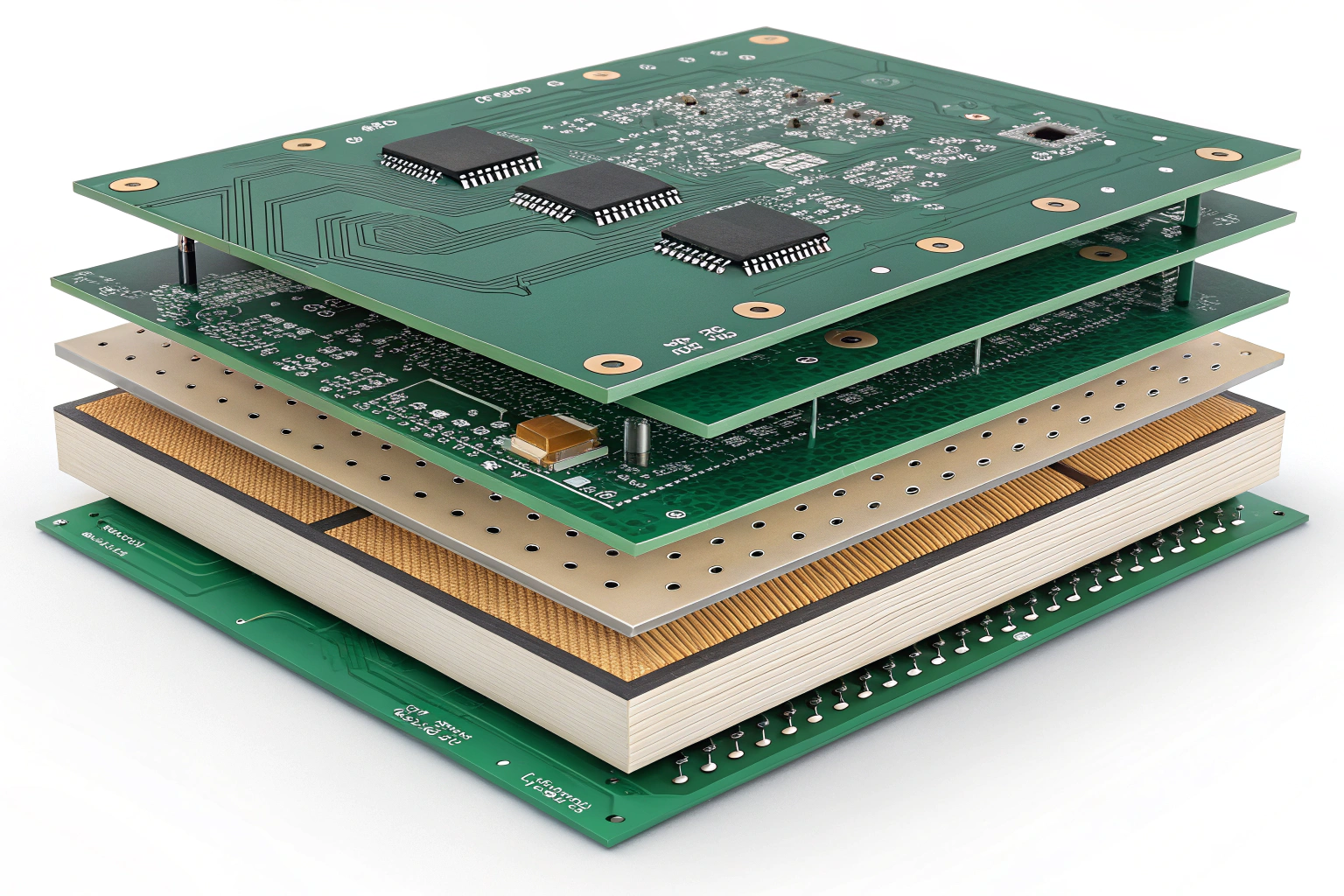
Before lamination, inner copper layers receive oxide or alternative surface treatment to improve adhesion with resin materials.
The lay-up process stacks materials in a precise order:
- Inner copper layers
- Prepreg sheets
- Core materials
- Outer copper foils
Alignment accuracy during lay-up directly affects annular ring quality, via reliability, and final electrical performance. Poor alignment at this stage leads to permanent defects embedded inside the board.
Lamination Pressing Process
Lamination bonds layers into one structure.
The stacked panels are placed into a lamination press, where controlled heat and pressure cure the resin and bond all layers into a single rigid board.
Key lamination controls include:
- Temperature profile and dwell time
- Pressure distribution
- Resin flow behavior
- Final board thickness and flatness
For higher layer counts or HDI designs, multiple lamination cycles may be required. Lamination quality has a direct impact on warpage, delamination resistance, and long-term structural stability.
Drilling, Desmear, and Via Preparation
Vertical interconnections are created.
After lamination, holes are drilled to form vias and component holes.
Drilling methods include mechanical drilling for standard vias and laser drilling for microvias. Drilling leaves resin smear on hole walls, which must be removed through desmear processing.
Clean hole walls are essential for strong copper adhesion during plating. Poor desmear is a common cause of via cracking and intermittent electrical failures in multilayer PCBs.
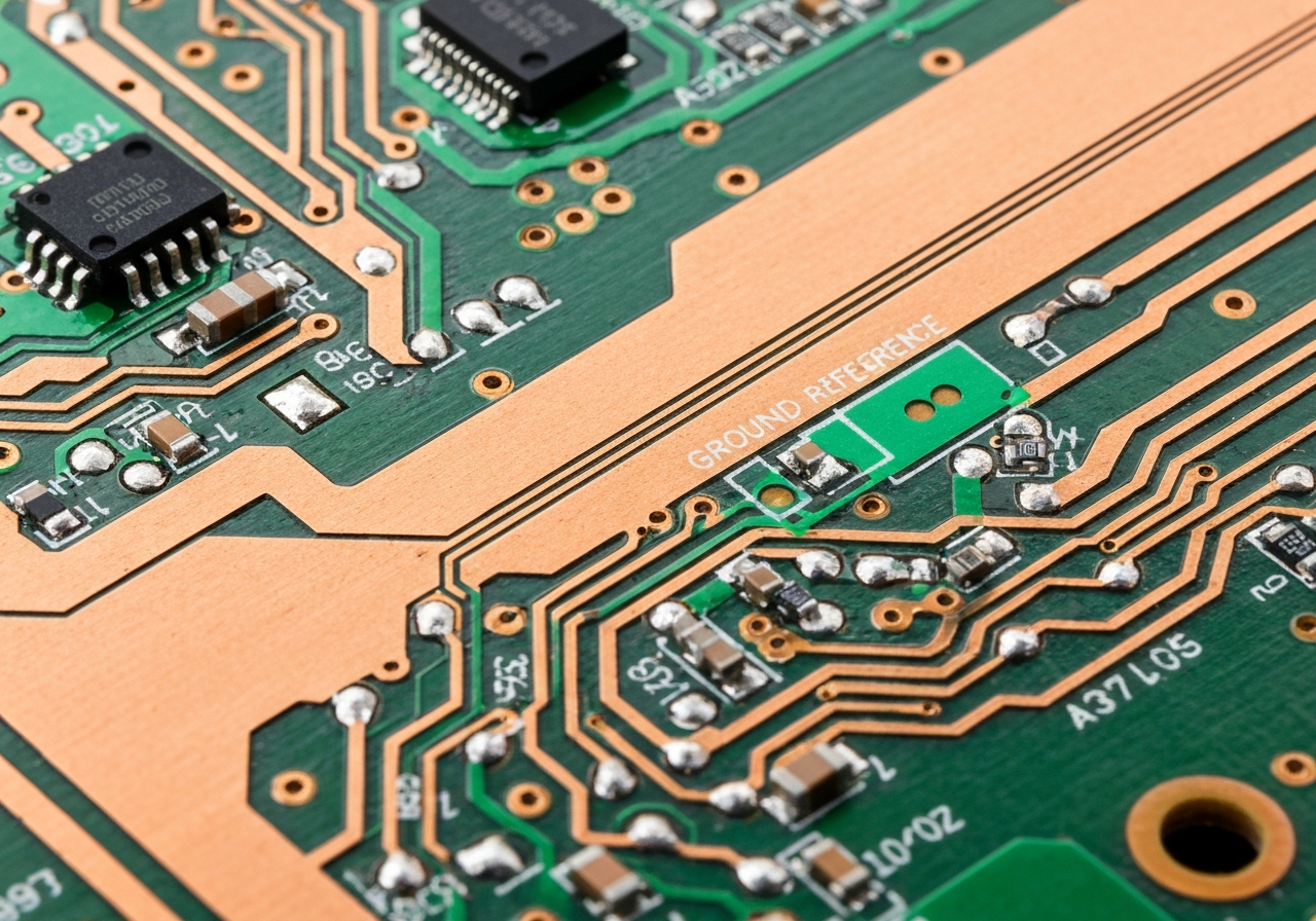
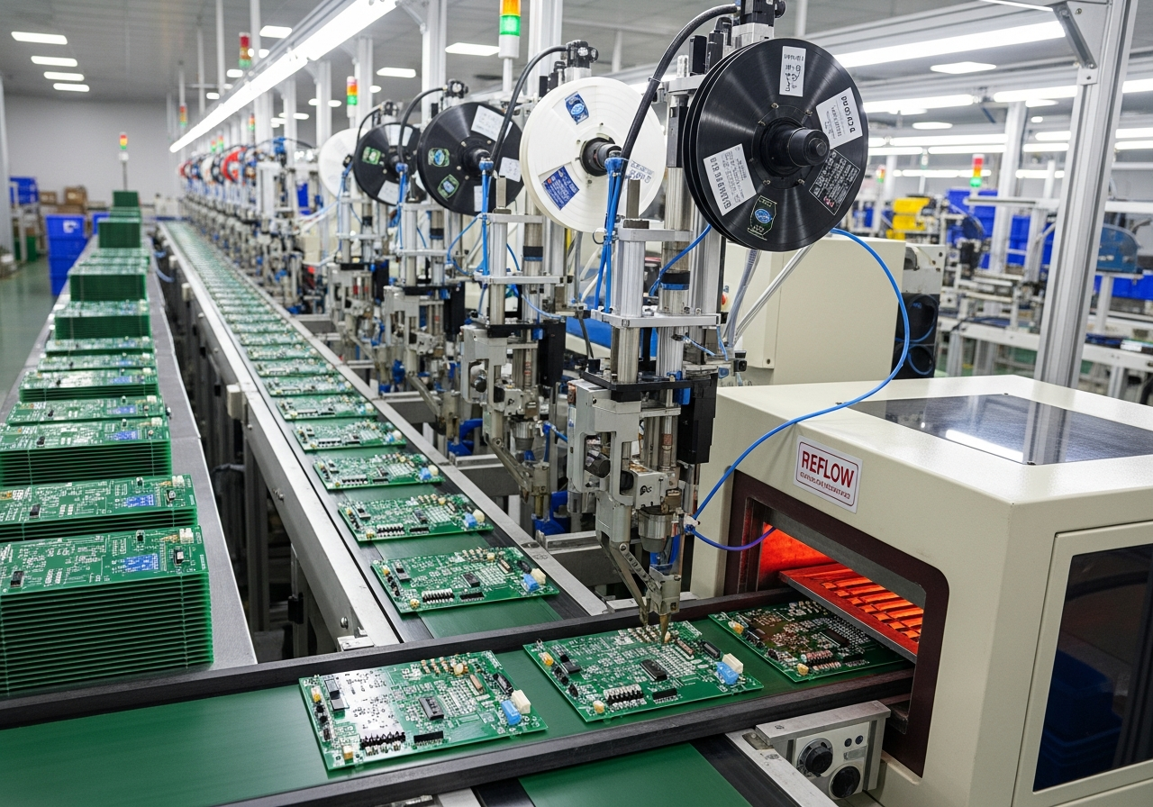
Copper Plating and Outer Layer Circuit Formation
Electrical continuity is completed.
A thin copper layer is first deposited chemically, followed by electroplating to build copper thickness on hole walls and outer layers.
After plating, outer layers are imaged and etched to form final surface circuits. AOI inspection is performed again to verify trace width, spacing, and pad integrity. This step is one of the most critical yield control points in fine-line multilayer designs.
Solder Mask, Surface Finish, and Profiling
Protection and solderability are added.
Solder mask is applied and cured to protect copper traces and control solder flow during assembly.
Common surface finishes include ENIG, lead-free HASL, and OSP. These finishes ensure good solderability and oxidation protection.
Boards are then routed or V-scored to define the final outline. Outline accuracy is essential for enclosure fit and downstream assembly processes.
Electrical Testing and Factory Quality Control
Testing verifies internal connectivity.
All multilayer PCBs undergo electrical testing to confirm continuity and isolation between nets.
Factory quality control typically includes:
- Electrical testing (flying probe or fixture-based)
- Visual inspection
- Thickness and dimensional measurement
- Process traceability records
For high-reliability applications, cross-section analysis may be used to verify internal layer alignment and plating thickness.
Conclusion
Multilayer PCB manufacturing is a structured, step-by-step process that builds electrical functionality layer by layer through controlled imaging, lamination, drilling, plating, and inspection. Each stage must be executed with precision, as errors at any point become embedded within the board and cannot be corrected later.
From a factory workshop perspective, stable multilayer PCB production relies on standardized stack-ups, mature lamination processes, and disciplined quality control systems. When inner-layer accuracy, lamination stability, and via reliability are well controlled, multilayer PCBs deliver high signal integrity, consistent assembly performance, and long-term durability. This combination of electrical performance and manufacturing consistency makes multilayer PCBs a core technology for modern electronic products requiring scalability, reliability, and predictable quality.
