
Printed circuit boards have evolved from simple single-sided layouts into complex multilayer structures. This change is driven by higher functional requirements, tighter space constraints, and stricter performance expectations. Multiple layers are not added for design complexity, but to achieve electrical stability, manufacturing consistency, and long-term reliability.
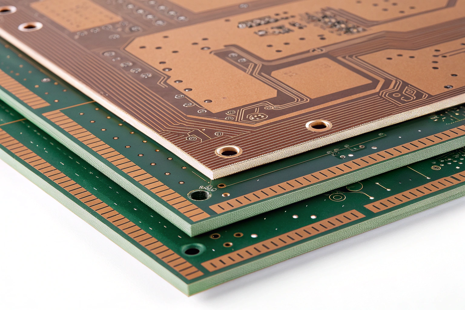
PCBs have multiple layers to increase routing capacity, improve signal integrity, stabilize power distribution, control EMI, reduce board size, and ensure reliable mass production.
Each added layer serves a clear electrical and process-related purpose.
Below are the main technical and manufacturing reasons why multilayer PCBs are widely used.
Why Do Multiple Layers Increase Routing Capacity?
Circuit complexity requires more space.
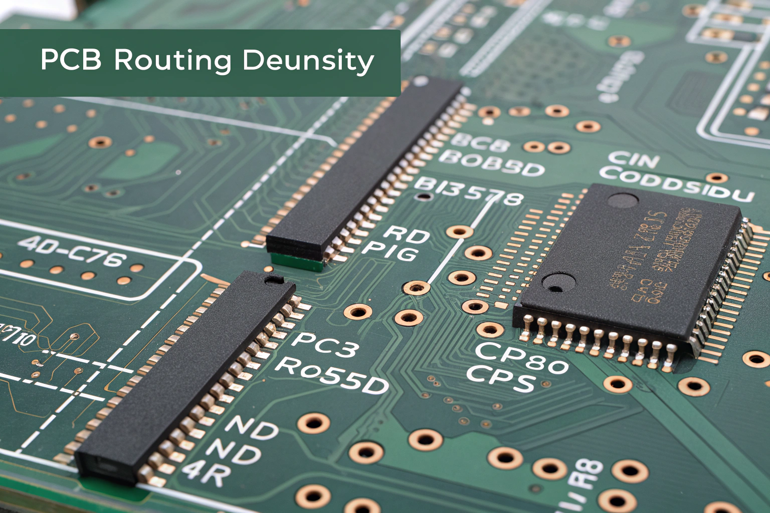
As component count increases, routing all signals on one or two copper layers becomes inefficient. Traces become longer, narrower, and more congested, increasing the risk of noise and layout errors.
Multilayer PCBs add internal signal layers that allow routing to be distributed vertically. This reduces trace length, avoids unnecessary crossovers, and keeps layouts clean and organized.
From a manufacturing standpoint, better routing distribution improves spacing control, reduces etching risk, and increases yield consistency during mass production.
Why Do Multilayer PCBs Improve Signal Integrity?
High-speed signals need controlled environments.
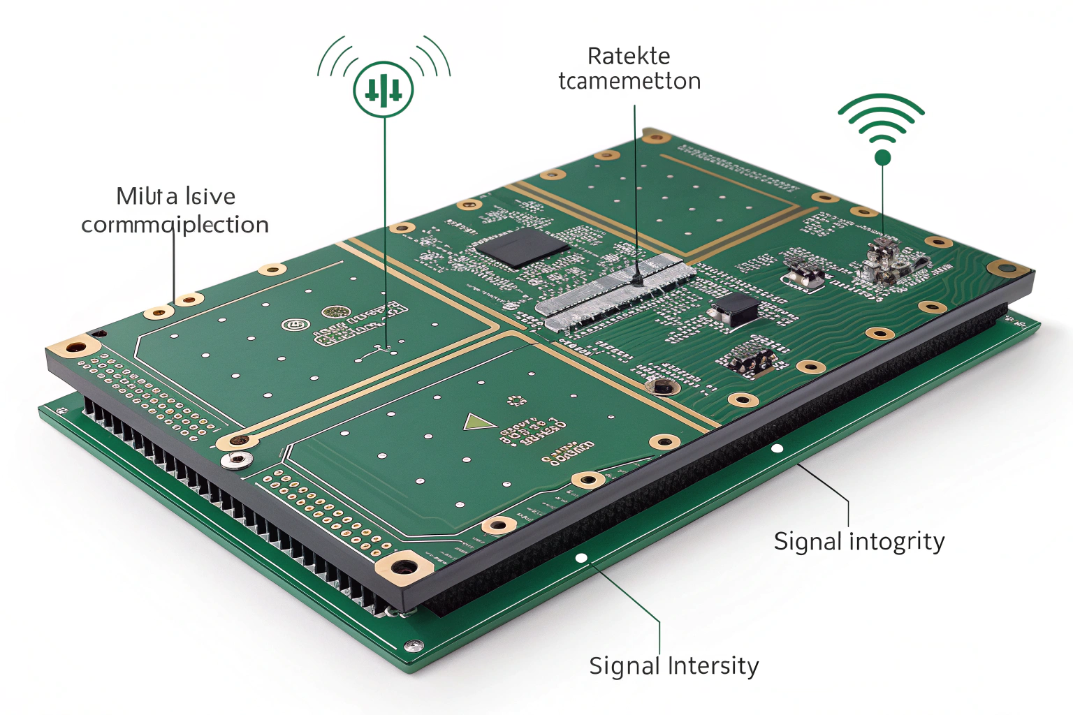
Modern circuits often include fast-switching processors, communication interfaces, and clock signals. These signals are sensitive to impedance changes, reflections, and crosstalk.
Multilayer PCBs allow signal layers to be placed adjacent to solid ground planes. This provides stable reference paths, short return loops, and controlled impedance. Compared to surface-only routing, internal signal layers show more predictable behavior across different production batches.
Stable signal integrity reduces functional variation during testing and improves overall product reliability.
Why Are Dedicated Power and Ground Layers Important?
Power stability affects every function.
In simple boards, power and ground are routed using narrow traces. As current demand increases, this approach leads to voltage drop, noise coupling, and uneven power distribution.
Multilayer PCBs typically include full copper planes dedicated to power and ground. These planes lower impedance, distribute current evenly, and improve decoupling capacitor effectiveness.
In factory testing environments, boards with solid power and ground planes show fewer intermittent failures and more stable functional results, especially under load changes.
Why Do Multiple Layers Help Control EMI and Noise?
EMI control starts inside the PCB.
Electromagnetic interference is often caused by large current loops, long signal paths, and poorly defined return paths.
Ground planes inside multilayer PCBs act as shields that confine electromagnetic fields and isolate noisy circuits from sensitive signals. Layer separation also allows noisy power circuits and low-level signals to be placed on different layers.
This structural EMI control reduces the need for external shielding and improves compliance with regulatory requirements.
Why Do Multilayer PCBs Enable Smaller Board Size?
More layers allow vertical integration.
By adding internal routing layers, more functionality can be packed into a smaller surface area.
This supports compact enclosures and higher functional integration. In manufacturing, smaller board outlines can improve panel utilization and reduce material waste, even when layer count increases.
Multilayer designs often achieve a better balance between size, performance, and production efficiency.
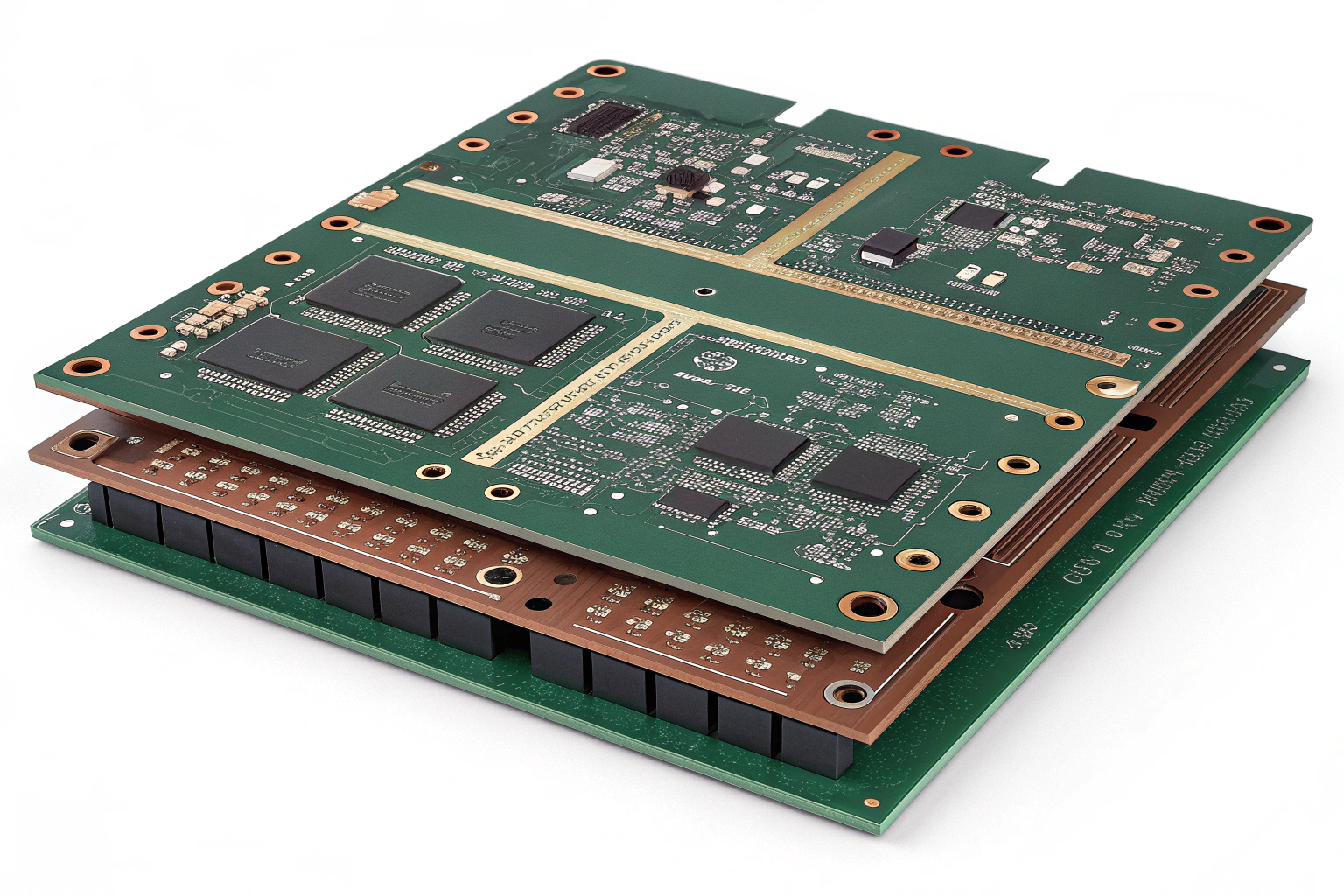
Why Are Multilayer PCBs Better for Manufacturing and Assembly?
Structure affects process stability.
Even-layer multilayer PCBs, such as four-layer designs, use symmetric stack-ups. This symmetry reduces internal stress during lamination and thermal cycles.
In factory workshops, balanced multilayer boards show:
- Less warpage during reflow soldering
- Better coplanarity for fine-pitch components
- More consistent solder joint quality
Standard multilayer stack-ups also fit well within mature manufacturing process windows, making quality easier to control from prototype builds to volume production.
How Do Factory Processes Support Multilayer PCBs?
Manufacturing discipline ensures reliability.
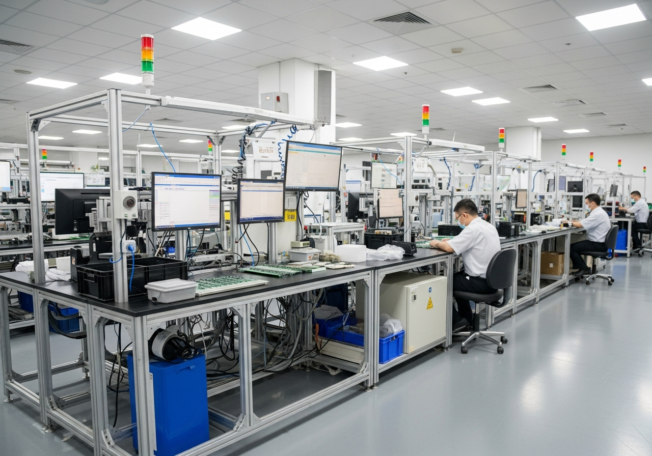
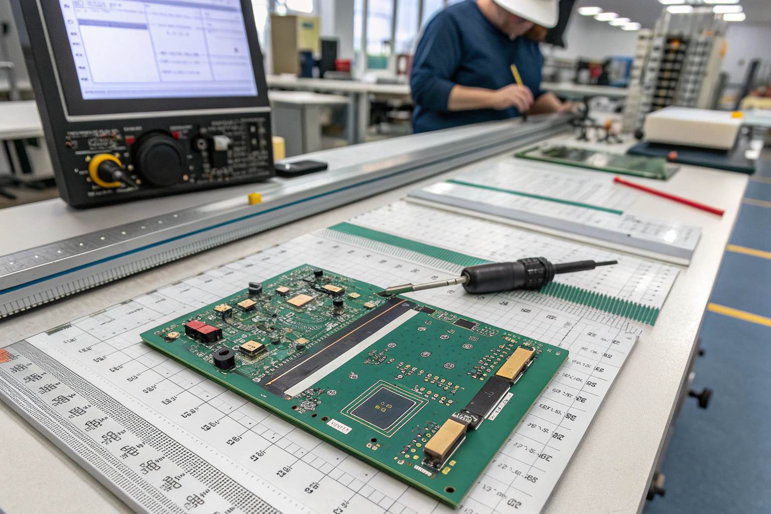
Producing multilayer PCBs requires controlled processes such as inner-layer imaging, lamination, drilling, plating, and inspection. Each step builds on the previous one.
Key process controls include:
- Inner-layer AOI before lamination
- Precise stack-up and alignment control
- Stable lamination pressure and temperature
- Via plating thickness monitoring
- Electrical testing and final inspection
These controls ensure that internal layers function as designed and remain reliable throughout the product lifecycle.
Conclusion
PCBs have multiple layers because modern electronic products demand higher routing density, stable signal behavior, reliable power delivery, and effective EMI control. Multilayer structures solve these challenges by distributing electrical functions across dedicated internal layers while maintaining mechanical balance.
From a manufacturing perspective, multilayer PCBs also provide more predictable assembly behavior, higher yield, and better long-term reliability. Although they involve more complex fabrication processes, standardized stack-ups and mature factory workflows make multilayer boards a practical and efficient solution. As product requirements continue to grow, multilayer PCBs remain a fundamental foundation for stable, scalable, and high-quality electronic manufacturing.
