
Testing whether a Printed Circuit Board (PCB) is faulty is a critical task in electronics manufacturing. A faulty PCB does not always fail completely. In many cases, the board powers on but behaves abnormally, shows unstable performance, or fails under specific conditions. If these issues are not identified early, they can lead to large-scale quality risks and costly rework.
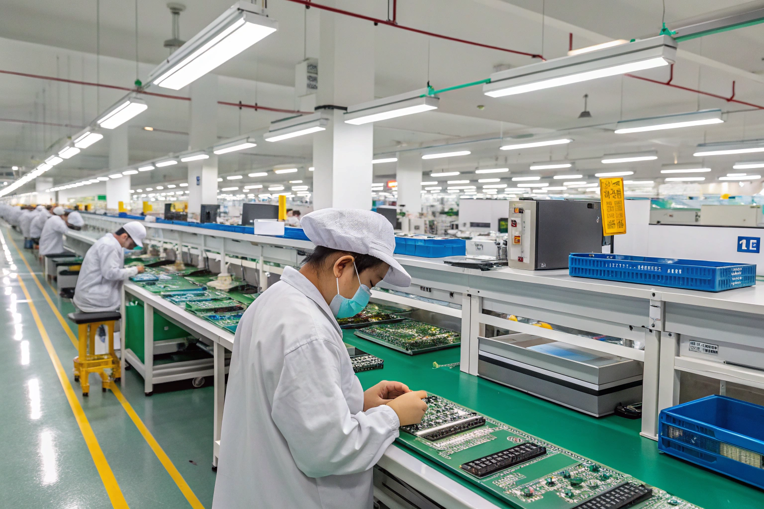
In professional manufacturing environments, PCB fault testing is not a single step. It is a structured system that combines inspection, electrical verification, functional validation, and process feedback. The following sections explain how faulty PCBs are identified through standardized testing methods used in factory workshops and production lines.
What Are the Early Signs of a Faulty PCB?
The first indication of a faulty PCB usually appears during initial inspection or early-stage testing. These signs help determine whether deeper electrical analysis is required.
Common early fault indicators include:
- Missing or misaligned components
- Poor solder joint appearance
- Discoloration or contamination on the PCB surface
- Warped boards or lifted pads
In manufacturing workshops, visual inspection is performed before any electrical power is applied. This step prevents further damage and filters out assembly-related defects. Automated Optical Inspection (AOI) systems are widely used after reflow soldering to detect placement errors, polarity issues, and solder defects.
Early detection at this stage significantly reduces downstream testing time and repair costs.
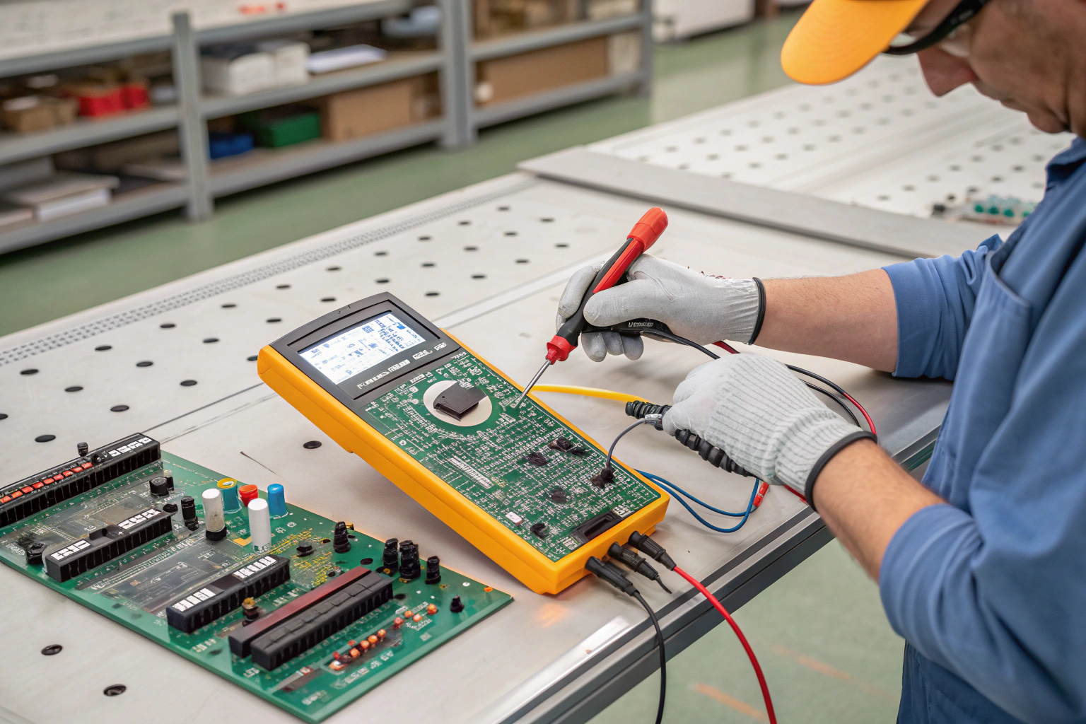
How Is Electrical Continuity Used to Detect PCB Faults?
After visual inspection, electrical continuity testing is used to confirm whether circuits are correctly connected.
Typical electrical checks include:
- Continuity testing for open circuits
- Short-circuit detection between power and ground
- Resistance measurement on critical nets
- Verification of reference voltages
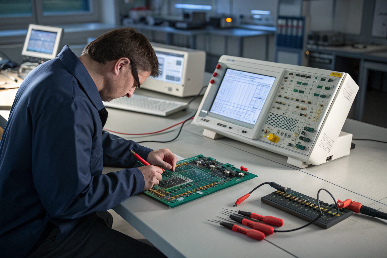
In factory environments, these tests are carried out using multimeters, flying probe testers, or dedicated In-Circuit Test (ICT) systems. ICT fixtures are especially effective for complex boards, as they can test thousands of nodes in seconds.
A PCB is classified as faulty if abnormal resistance values, unexpected shorts, or open connections are detected. Electrical continuity testing provides objective data and forms the foundation of fault isolation.
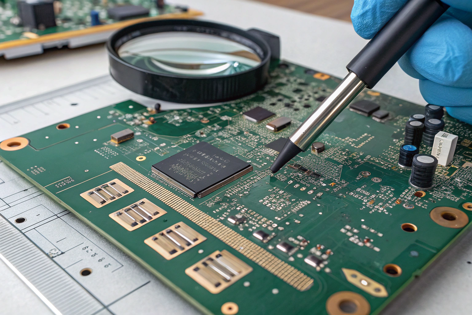
How Does In-Circuit Testing Identify Assembly Faults?
In-Circuit Testing focuses on individual components and solder joints rather than overall board function. This method is essential for detecting hidden or non-obvious faults.
ICT typically verifies:
- Component presence and value
- Orientation of diodes and transistors
- Pin-level connectivity
- Basic IC response
In SMT workshops, ICT test points are planned during the design phase to ensure sufficient coverage. Poor test access often results in undetected faults and delayed troubleshooting.
ICT results are recorded and analyzed by engineering teams. Repeated failures at the same nodes usually indicate process issues such as solder paste printing instability or placement accuracy drift.
How Is Functional Testing Used to Confirm PCB Faults?
Functional testing determines whether the PCB performs its intended function under real operating conditions. This step often reveals faults that electrical tests cannot detect.
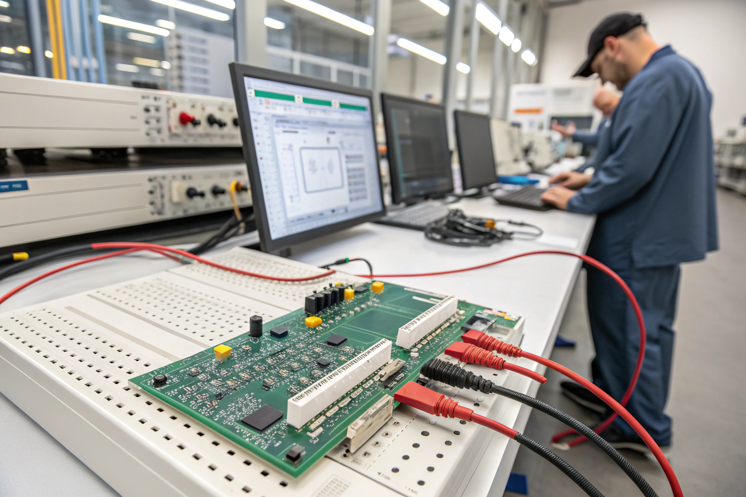
Functional testing may include:
- Power-up sequence verification
- Signal input and output validation
- Communication interface testing
- Load and stress simulation
In manufacturing workshops, Functional Circuit Test (FCT) stations simulate the actual application environment. Custom fixtures, firmware, and software tools are used to validate performance.
A PCB is considered faulty if it fails to meet defined functional criteria, even if it passes continuity and ICT checks. Functional testing bridges the gap between electrical correctness and real-world operation.
How Do Factory Processes Influence PCB Fault Detection?
The accuracy of fault testing depends heavily on manufacturing process control. Testing effectiveness increases when it is integrated into the production workflow.
Key process factors include:
- Stable SMT placement accuracy
- Controlled solder paste printing
- Optimized reflow temperature profiles
- ESD-safe handling and storage
In professional workshops, testing stations are positioned at critical points along the production line. AOI is placed after reflow, while ICT and FCT are performed after final assembly.
Test yield data is continuously reviewed by process and quality teams. Abnormal failure trends often trigger immediate process audits and corrective actions, ensuring faults are addressed at the source.
How Is Fault Analysis and Retesting Performed?
Once a PCB is identified as faulty, it enters a controlled fault analysis and rework process.
Standard steps include:
- Failure symptom documentation
- Root cause analysis by engineering teams
- Controlled rework or component replacement
- Full retesting and validation
- Process improvement feedback
Rework is performed in dedicated areas using temperature-controlled tools and ESD protection. Random or undocumented fixes are avoided. Each repaired PCB must pass the same testing standards as a new board.
Fault data is used to refine design guidelines, assembly processes, and testing strategies, reducing future defect rates.
Conclusion
Testing whether a PCB is faulty is a comprehensive engineering activity that combines inspection, electrical verification, functional testing, and manufacturing process control. A faulty PCB is not just a defective unit but a signal of potential weaknesses in design, materials, or production processes. Through structured testing systems, disciplined workshop operations, and continuous data analysis, manufacturing environments can identify PCB faults early and prevent them from spreading into large-scale quality issues. A mature testing strategy transforms fault detection into a powerful tool for long-term reliability and stable production performance.
