
A PCB switch is a critical interface component that directly affects product usability and electrical reliability. When a PCB switch fails, the entire device may appear unresponsive even if other circuits function correctly. In manufacturing environments, PCB switch testing is treated as both an electrical verification task and a process quality checkpoint.
Testing a PCB switch is not limited to pressing the button and observing a response. Professional testing combines visual inspection, electrical measurement, functional validation, and process review. The following sections explain how PCB switches are tested systematically in factory workshops and controlled production lines.
What Is a PCB Switch and Why Does It Need Testing?
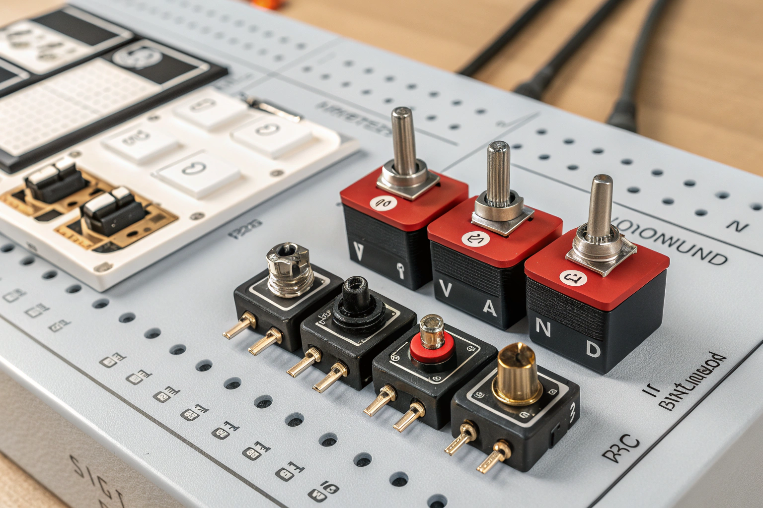
A PCB switch is a mechanical or electromechanical component mounted on a printed circuit board to control circuit states. Common types include tactile switches, slide switches, toggle switches, and membrane switches.
PCB switch testing is necessary to verify:
- Correct mechanical movement
- Stable electrical contact
- Proper solder joint quality
- Consistent performance over repeated use
In manufacturing, switches are high-touch components. Even minor defects can lead to intermittent contact, false triggering, or complete failure after short-term use. For this reason, switch testing is integrated into both assembly inspection and functional testing stages.
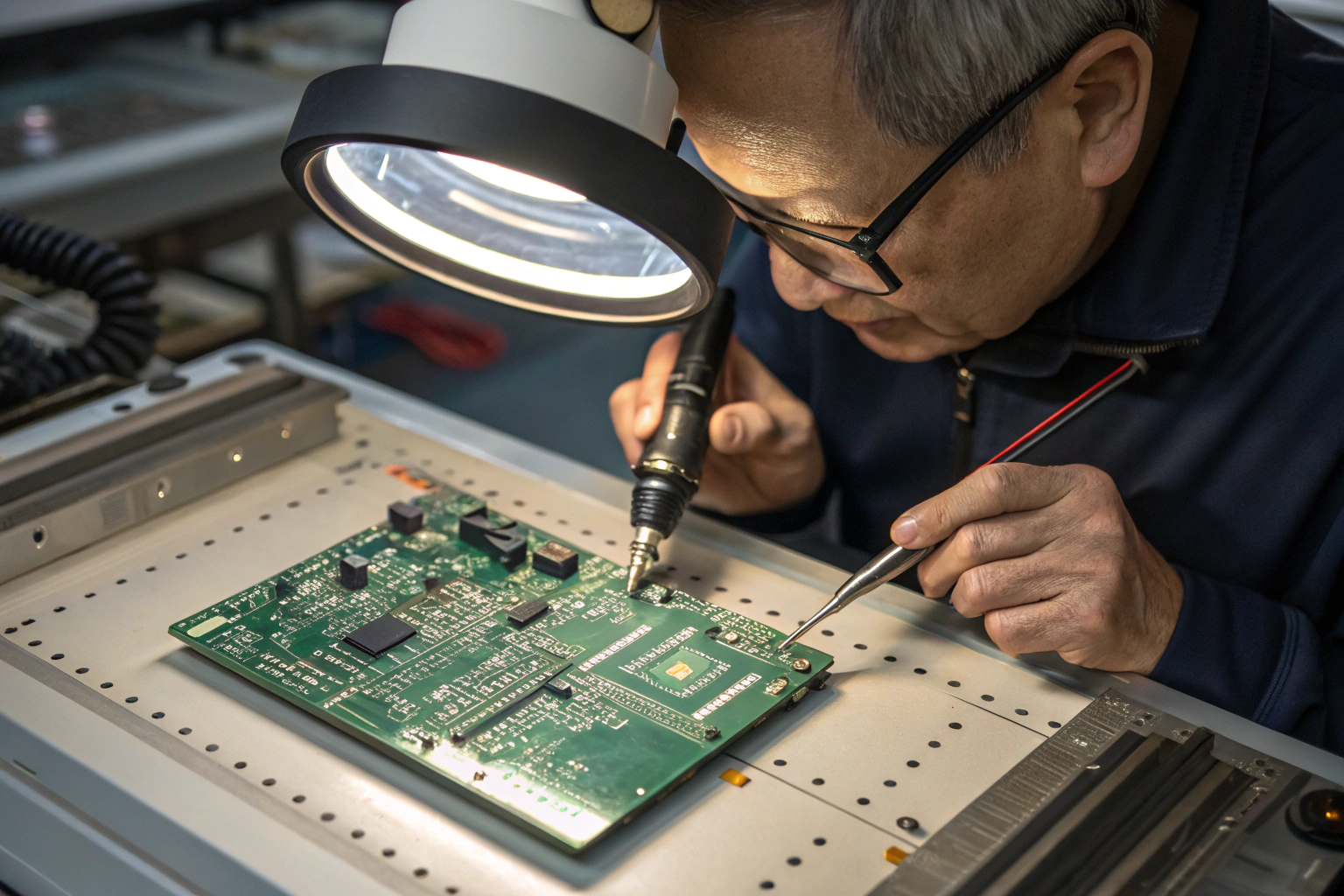
How Is Visual Inspection Used to Check PCB Switches?
Visual inspection is the first step in PCB switch testing and often reveals assembly-related issues.
Inspection points include:
- Switch alignment and seating on the PCB
- Solder joint shape and wetting
- Presence of solder bridges or cold joints
- Damage to switch housing or actuator
In SMT workshops, visual inspection is supported by magnification tools or Automated Optical Inspection (AOI) systems. AOI checks switch placement accuracy and solder quality after reflow soldering.
Improperly seated switches may still pass electrical tests initially but fail after repeated operation. Visual inspection helps detect these risks early and prevents unreliable boards from entering later production stages.
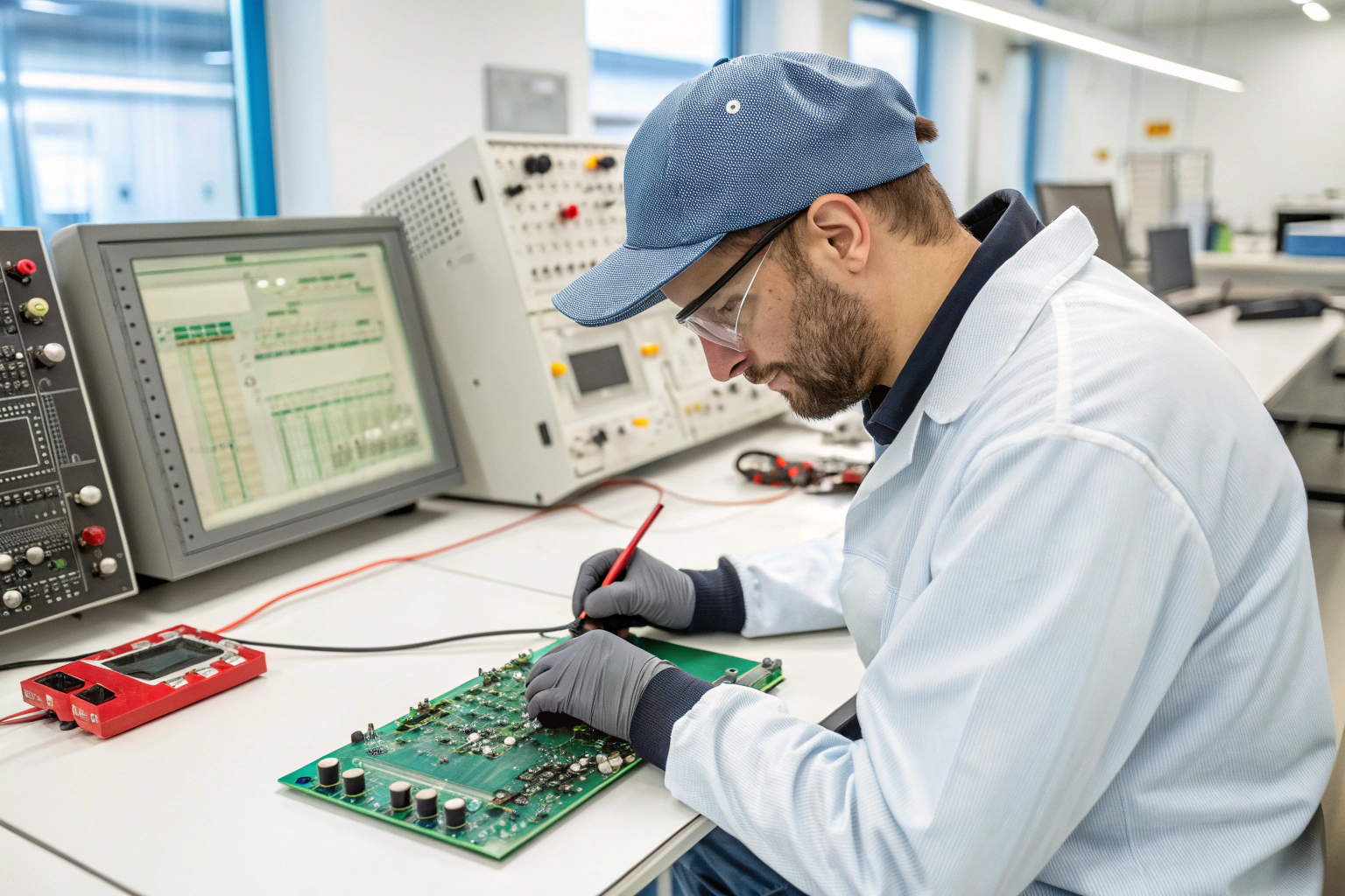
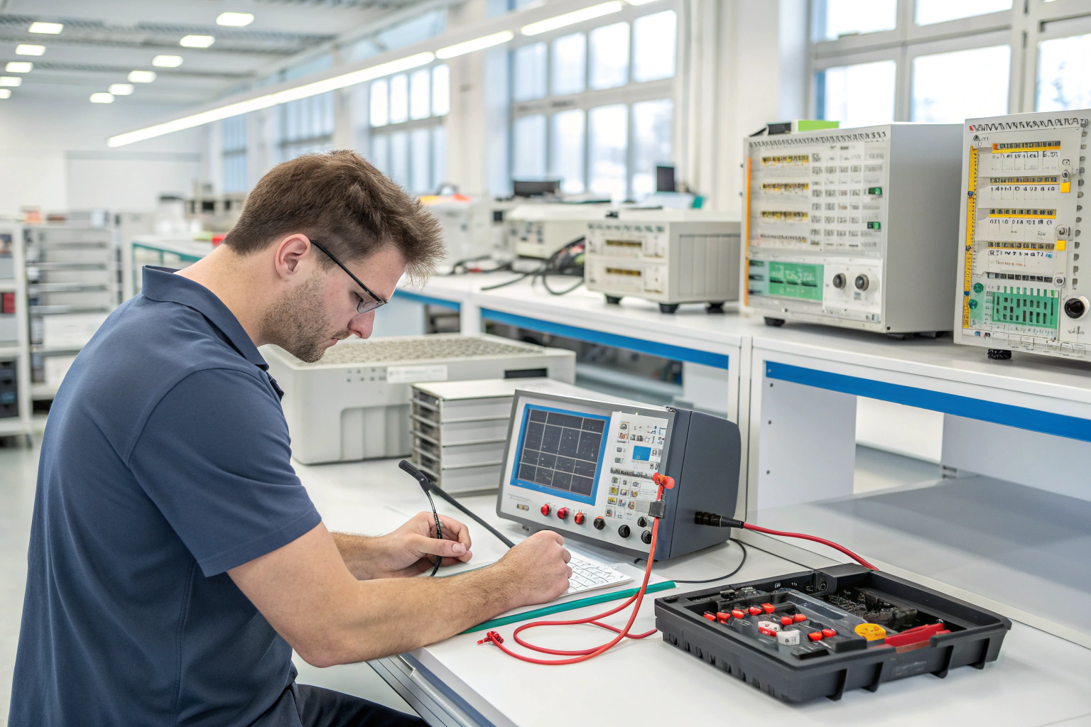
How Is Electrical Continuity Used to Test a PCB Switch?
Electrical continuity testing confirms whether the switch correctly opens and closes the circuit as designed.
Typical electrical tests include:
- Measuring resistance across switch terminals
- Verifying open and closed states
- Checking for unstable or fluctuating readings
In factory environments, multimeters or automated test fixtures are used. When the switch is not pressed, resistance should indicate an open circuit. When pressed or toggled, resistance should drop to near zero, indicating proper contact.
Abnormal resistance values often indicate internal switch damage, solder joint defects, or contamination. Electrical continuity testing provides objective data and is essential for identifying intermittent switch faults.
How Is Functional Testing Performed on PCB Switches?
Functional testing verifies that the switch performs its intended role within the circuit under real operating conditions.
Functional checks may include:
- Triggering system responses through the switch
- Verifying debounce behavior in firmware
- Confirming correct signal logic levels
- Testing switch response speed and consistency
In manufacturing workshops, Functional Circuit Test (FCT) stations simulate actual product operation. Switches are pressed repeatedly while monitoring system output, display response, or communication signals.
This stage often reveals issues that simple continuity tests cannot detect, such as timing instability or weak contact under load. Functional testing ensures that the switch works reliably within the full system context.
How Do Assembly Processes Affect PCB Switch Performance?
PCB switch reliability is strongly influenced by assembly process quality.
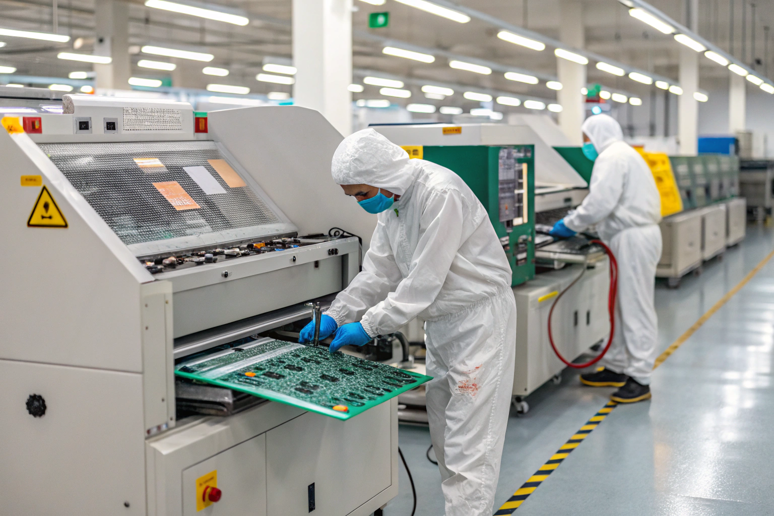
Key process factors include:
- Solder paste volume control
- Placement pressure and alignment
- Reflow temperature profile stability
- Mechanical stress during depaneling
In SMT workshops, incorrect solder paste thickness can cause insufficient solder joints or excessive solder that affects switch movement. Excessive placement force may deform the switch body, while improper reflow profiles can weaken internal contacts.
Manufacturing engineers monitor these parameters closely. When switch failures occur, process data such as stencil design, placement force settings, and reflow curves are reviewed to identify root causes.
How Is Durability and Reliability of PCB Switches Verified?
Beyond initial functionality, PCB switches must withstand repeated use over the product’s lifetime.
Reliability testing may include:
- Repeated actuation cycle testing
- Environmental exposure testing
- Vibration or mechanical stress testing
- Long-duration functional operation
In manufacturing environments, sample boards may undergo life-cycle testing to evaluate switch durability. Weak switches often fail during early cycles, revealing quality or supplier issues.
Test results are documented and used to refine component selection, assembly parameters, and quality standards. This approach reduces field failure risk and improves long-term product stability.
Conclusion
Testing a PCB switch is a structured manufacturing process that goes far beyond basic operation checks. It combines visual inspection, electrical continuity measurement, functional validation, and process control within the factory workshop. A properly tested PCB switch ensures stable electrical contact, consistent user interaction, and long-term reliability. By integrating switch testing into assembly, testing, and quality systems, manufacturing operations can prevent intermittent failures, reduce rework, and deliver more dependable electronic products.
