
Surface Mount Technology (SMT) has transformed electronics manufacturing—but how exactly does the SMT assembly procedure work, and how can it help you build better, more reliable devices?
The SMT assembly process includes applying solder paste, placing components, reflow soldering, and inspection. Mastering each stage is key to producing high-quality circuit boards efficiently and accurately.
In modern electronics, SMT (Surface Mount Technology) is the backbone of high-density, high-speed, and compact device design. From smartphones to medical sensors, SMT allows manufacturers to mount components directly onto the surface of a PCB (Printed Circuit Board), eliminating the need for drilling holes or using bulky parts.
But to fully benefit from SMT, you need to understand each step in the process—from paste to placement, from soldering to inspection. This article walks you through the complete SMT assembly flow and shows how refining your knowledge of each stage helps reduce defects, improve quality, and accelerate time-to-market.
What Is SMT Assembly?
SMT assembly is the method of mounting electronic components directly onto the surface of a printed circuit board. Unlike traditional through-hole technology (THT), which requires drilling holes for component leads, SMT components are much smaller and allow for higher component density.
In an SMT line, most of the process is automated, using robotic machines for precise placement, ovens for reflow soldering, and inspection tools to ensure quality. The result? Smaller, lighter, and faster electronic products.
If you’re developing modern electronics, choosing SMT over THT can dramatically improve board design, reduce size, and increase speed. Learn more about this difference in this detailed comparison from Tempo Automation.
Step-by-Step SMT Assembly Procedure
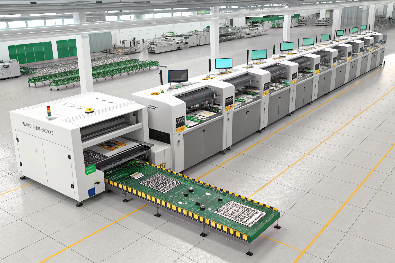
While exact steps can vary by factory or product, the standard SMT process usually includes:
1. Solder Paste Printing
Solder paste, a mix of metal alloy and flux, is applied to PCB pads using a stencil. This forms the base for connecting each component.
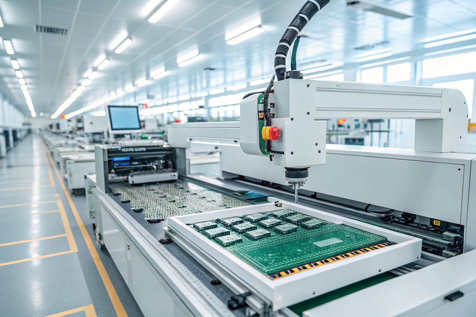
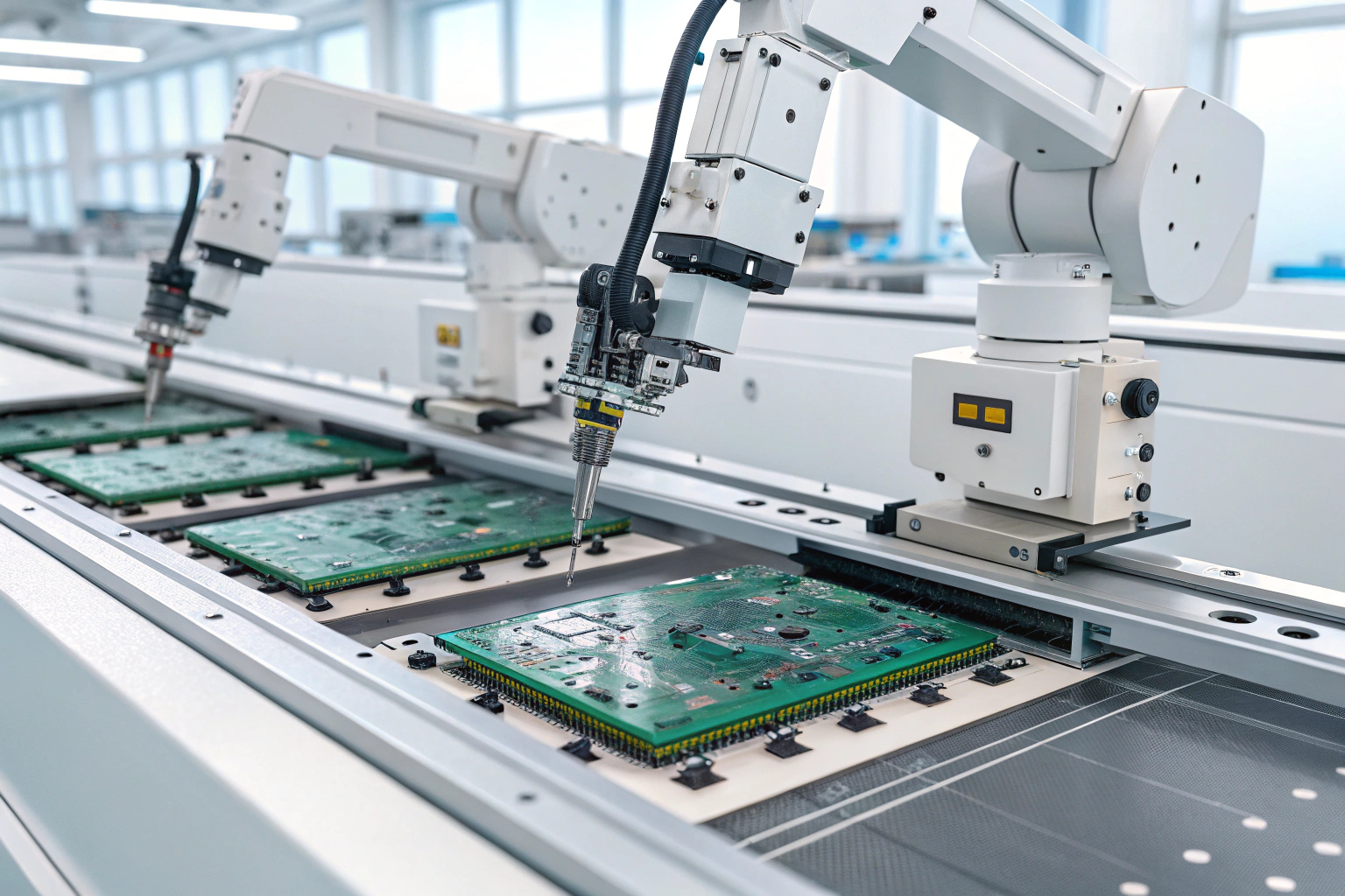
2. Pick-and-Place Component Mounting
High-speed machines accurately place each component on top of the solder paste. This step handles everything from resistors and capacitors to ICs and BGAs.
3. Reflow Soldering
The PCB is passed through a reflow oven, which gradually heats the board to melt the solder paste and bond each component to its pad. Precise temperature profiles are critical here.
4. Inspection and Quality Control
After soldering, the board undergoes AOI (Automated Optical Inspection) or X-ray inspection (for BGA components) to check for placement errors, soldering defects, and shorts.
For complex or high-reliability boards, additional functional testing or ICT (In-Circuit Testing) is used.
Each step must be perfectly aligned with your board’s design file. Want a visual breakdown of the reflow process? Check out Eurocircuits’ step-by-step SMT overview.
Why SMT Improves Electronic Product Design
Using SMT assembly offers a host of design and production advantages:
- Smaller PCB size due to compact components and denser layout
- Lower production cost through automation and material efficiency
- Higher performance due to shorter signal paths and better EMI control
- Greater scalability from prototype to mass production
These benefits make SMT ideal not just for big brands but also for startups and innovators who need to pack more functionality into smaller form factors.
With SMT, it’s possible to move from a functional prototype to a scalable product line with minimal redesign—especially when working with a manufacturing partner that offers DFM (Design for Manufacturability) services.
Common SMT Assembly Issues and How to Avoid Them
Even with automation, SMT isn’t foolproof. Here are some typical issues and how to prevent them:
- Solder Bridging – Caused by excess paste or poor stencil design. Use precise stencil thickness and print pressure.
- Component Misalignment – Often results from vibration or paste slumping. Make sure placement machines are calibrated and boards are handled properly.
- Tombstoning – Happens when one side of a component lifts off during reflow. Controlled temperature profiles can reduce this.
- Cold Solder Joints – Caused by incomplete reflow. Use quality solder paste and proper reflow profiles.
Early involvement with an experienced CM (Contract Manufacturer) can help minimize these problems. See Sierra Circuits’ SMT checklist to ensure defect-free builds.
Conclusion
Understanding the full SMT assembly procedure empowers you to build better electronics—from development to volume production. With accurate solder paste printing, precise placement, careful reflow, and thorough inspection, you can dramatically improve yield, quality, and consistency in your builds.
Whether you’re launching a new IoT product, designing wearable tech, or scaling up for mass production, mastering SMT is one of the smartest moves you can make. Choose the right partners, design with manufacturability in mind, and let automation do the heavy lifting.
