
PCB layer count usually follows even numbers such as 2, 4, 6, or more. This leads to a common question during early design review: whether a 3 layer PCB is technically possible and practical for manufacturing.
Yes, a 3 layer PCB can be made, but it is rarely used and generally not recommended for standard production.
Although feasible from a technical standpoint, it introduces structural imbalance, process complexity, and reliability risks.
Understanding why 3 layer PCBs are uncommon helps clarify standard PCB design rules and manufacturing decisions.
Is a 3 Layer PCB Technically Possible?
Physics does not prevent it, but process logic does.
From a purely technical perspective, a PCB with three copper layers can be fabricated. One outer layer, one inner layer, and the opposite outer layer can be laminated together.
However, PCB manufacturing is based on symmetric lamination. Even-layer stack-ups naturally balance internal stress during pressing and thermal cycling. A 3 layer structure breaks this symmetry, making the board more prone to warpage and delamination.
For this reason, most PCB fabrication standards do not treat 3 layers as a normal configuration, even though it is not forbidden.
Why Are PCB Layers Usually Even Numbers?
Balance is the core reason.
PCB lamination uses heat and pressure to bond copper layers and dielectric materials together. Symmetric stack-ups distribute mechanical stress evenly across the board.
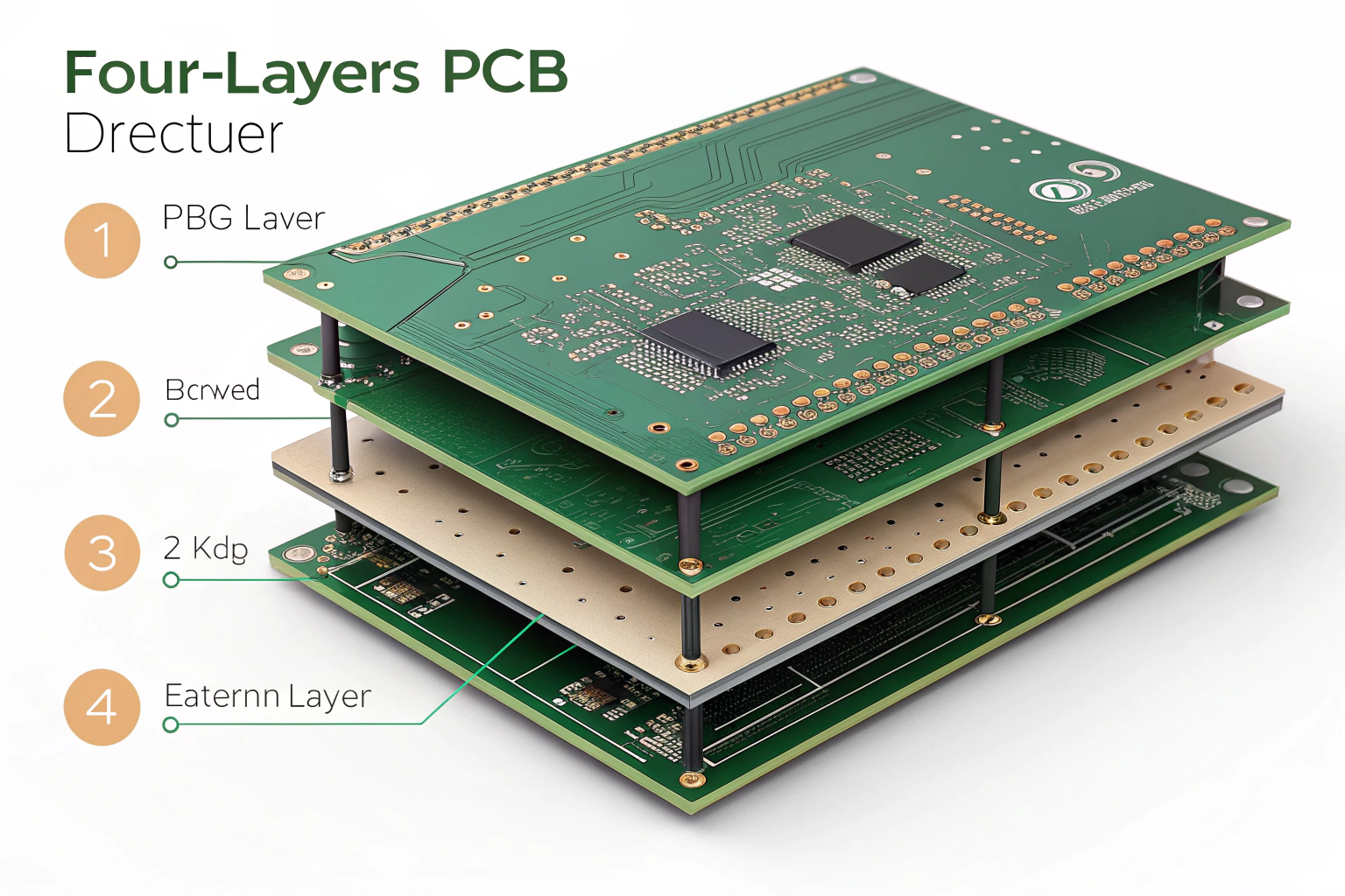
Even-layer boards such as 4-layer PCBs typically use a mirrored structure:
- Top signal layer
- Inner plane or signal layer
- Inner plane or signal layer
- Bottom signal layer
This symmetry minimizes warpage during fabrication, reflow soldering, and long-term use. A 3 layer PCB lacks this balance, which increases deformation risk during assembly and temperature changes.
In production workshops, warped boards create placement accuracy issues, solder defects, and test fixture alignment problems.
What Would a 3 Layer PCB Stack-Up Look Like?
The structure is inherently unbalanced.
A typical 3 layer PCB stack-up may look like:
- Top copper layer
- Dielectric
- Inner copper layer
- Dielectric
- Bottom copper layer
The inner copper layer is not centered relative to the board thickness, which causes uneven thermal expansion. During reflow soldering, this imbalance can lead to board bowing or twisting.
Manufacturers can attempt to compensate using special prepreg thickness or copper balancing, but this increases engineering effort and cost while still offering lower reliability than a standard 4-layer board.
Why Is a 4 Layer PCB Preferred Over a 3 Layer PCB?
The jump from 3 to 4 layers solves multiple problems.
A 4 layer PCB provides:
- Structural symmetry
- Dedicated power and ground planes
- Better signal integrity
- Lower EMI risk
From a cost perspective, the difference between producing a 3 layer and a 4 layer PCB is often minimal. Lamination, drilling, and inspection steps are already required, and adding one more layer does not double the complexity.
In manufacturing environments, standard 4-layer stack-ups are well-documented, stable, and repeatable. Process windows are wider, yield is higher, and long-term reliability is easier to guarantee.
For these reasons, most engineers move directly from 2 layers to 4 layers rather than attempting a 3 layer solution.
Are There Any Special Cases Where a 3 Layer PCB Is Used?
Only in very limited or experimental scenarios.
3 layer PCBs may appear in:
- Research or academic experiments
- Highly customized legacy designs
- Cost-driven redesigns with extreme constraints
Even in these cases, manufacturers usually recommend redesigning the board into either a 2-layer or 4-layer structure. The risk introduced by mechanical imbalance often outweighs any theoretical benefit.
In production workshops, non-standard stack-ups increase communication overhead, slow engineering approval, and raise the chance of errors during fabrication and assembly.
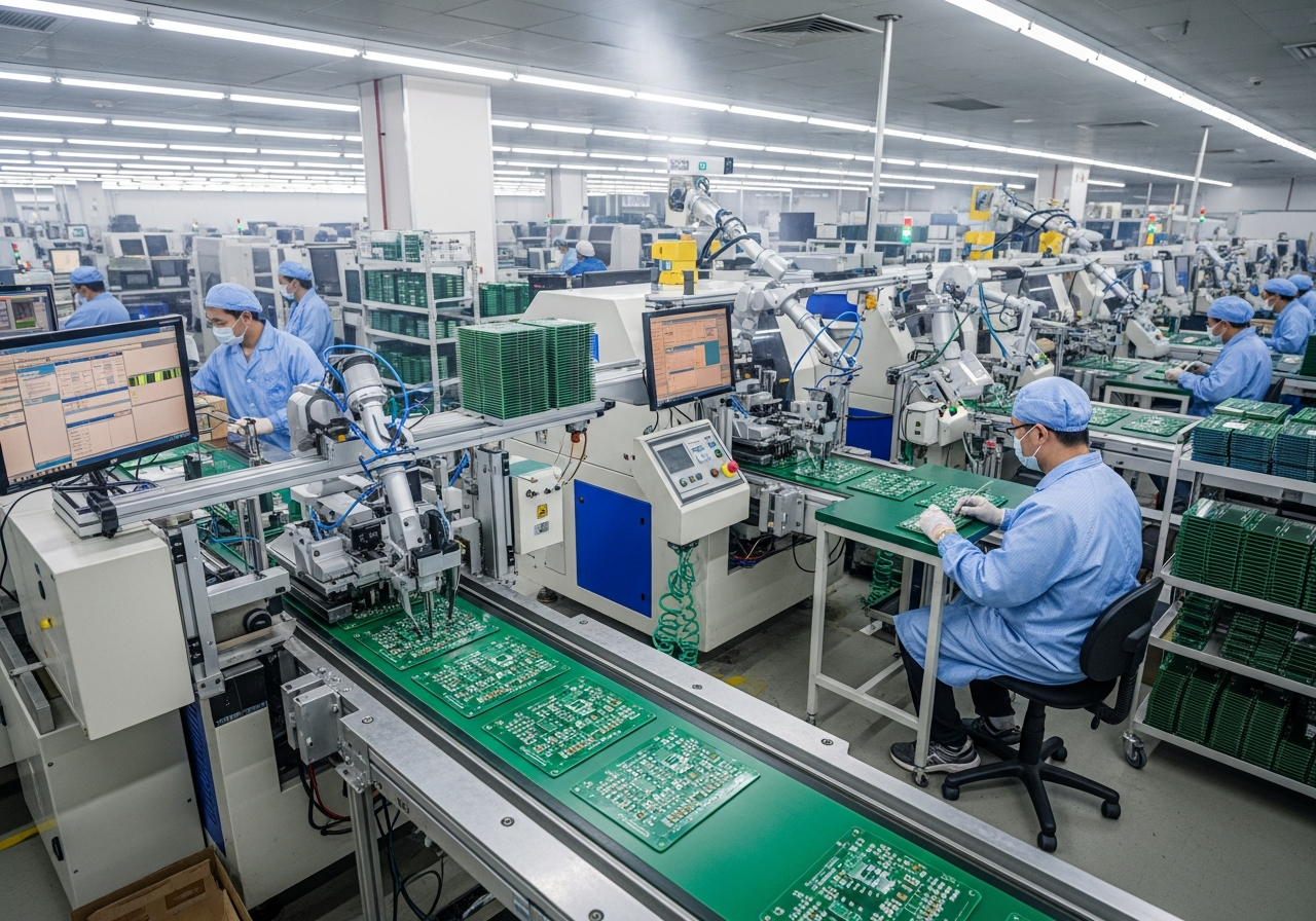
How Does a 3 Layer PCB Affect Assembly and Workshop Processes?
Manufacturing difficulty increases noticeably.
During SMT assembly, a 3 layer PCB is more sensitive to heat distribution. Uneven copper density across layers can cause localized bending during reflow soldering.
Warped boards affect:
- Solder joint quality
- Component coplanarity
- AOI inspection accuracy
- Functional test reliability
Fixtures may require additional support pins, and process windows become narrower. These adjustments add time and reduce overall production efficiency.
From a quality control perspective, maintaining consistency across batches becomes more challenging compared to standard even-layer boards.
Conclusion
A 3 layer PCB is technically possible, but it sits outside normal industry practice. The core issue is not feasibility, but stability. An uneven stack-up introduces mechanical stress, higher warpage risk, and tighter process limits during fabrication and SMT assembly. These risks become more visible as production volume increases and environmental conditions vary.
In practical manufacturing, standardization is critical. Even-layer PCBs, especially 4-layer designs, offer balanced structures, predictable lamination behavior, and mature process control. They support better signal integrity, easier testing, and more consistent quality across batches. Compared with the marginal theoretical benefit of a 3 layer board, the trade-offs in reliability and process complexity are significant.
For these reasons, most engineering and manufacturing teams avoid 3 layer PCBs in favor of well-established 2-layer or 4-layer solutions. This approach reduces production uncertainty, improves assembly yield, and ensures long-term product stability in real-world operating conditions.
