
Electrostatic discharge (ESD) is the sudden flow of electrical charge between two objects, capable of damaging sensitive electronic components during handling and assembly.

Understanding ESD is essential for preventing hidden defects, reducing failure rates, and ensuring stable quality throughout prototype and mass-production builds.
Why does ESD matter so much in electronics manufacturing?
Uncontrolled ESD events often cause latent damage, reduced component lifespan, or complete device failure.
ESD protection prevents static charge from harming sensitive semiconductor devices during production.
Charge Build-Up, Component Sensitivity, and Hidden Failures
ESD occurs when static charge accumulates on surfaces like clothing, tools, or PCBs. When discharged, even a few volts can degrade microchips. Components such as MOSFETs, ICs, RF modules, and sensor interfaces are extremely sensitive to electrostatic energy. Damage can be immediate or latent, causing intermittent failures in the field.
Engineering-aligned factories apply standardized ESD controls, monitor handling areas, and verify component sensitivity. With integrated PCB assembly, testing, and packaging workflows, ESD risks are minimized from the moment materials enter the production floor.
How does ESD occur during manufacturing processes?
Static charge builds easily during handling, packaging, and board movement on assembly lines.
ESD occurs when accumulated charge transfers between people, tools, or surfaces and the electronic components.
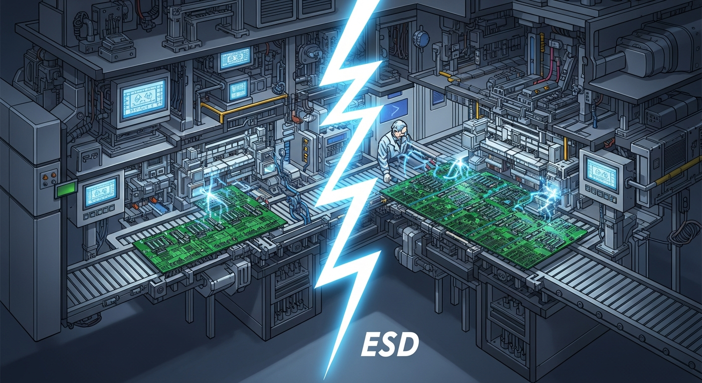
Friction, Induction, and Direct Contact
Common sources include friction from conveyor belts, packaging materials, solder mask surfaces, and operator clothing. Induced charging happens when components pass near charged objects. Direct discharge occurs when a tool or human hand contacts sensitive leads or pads.
Factories evaluate environmental factors such as humidity, workstation materials, and movement patterns. Engineering teams implement best practices to reduce opportunities for charge accumulation during SMT placement, wave soldering, testing, and packaging.
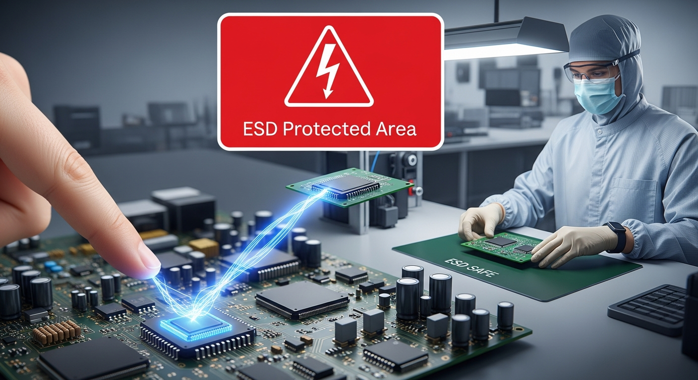
What ESD protection measures are used in manufacturing lines?
Weak ESD control leads to irreversible IC damage, unstable prototypes, and high reject rates.
ESD protection uses grounded equipment, controlled environments, and anti-static materials to prevent charge build-up.
EPA Zones, Grounding, and Anti-Static Tools
Key protection methods include:
- EPA (ESD Protected Areas) with grounded workstations
- Wrist straps and heel straps to discharge human body charge
- Conductive mats and floors to control surface charge
- Ionizers to neutralize air-borne static
- Anti-static gloves, bins, and bags to protect components
- Proper grounding of pick-and-place and testing equipment
Manufacturing partners with IPC-ESD standards maintain continuous monitoring logs, calibrate ESD equipment, and document preventative actions. This reduces ESD-related defects and supports consistent production yields.
How does ESD impact PCB assembly and long-term reliability?
ESD damage is often invisible during assembly but causes failures months later.
ESD can weaken semiconductor junctions, degrade insulation, and reduce device endurance.
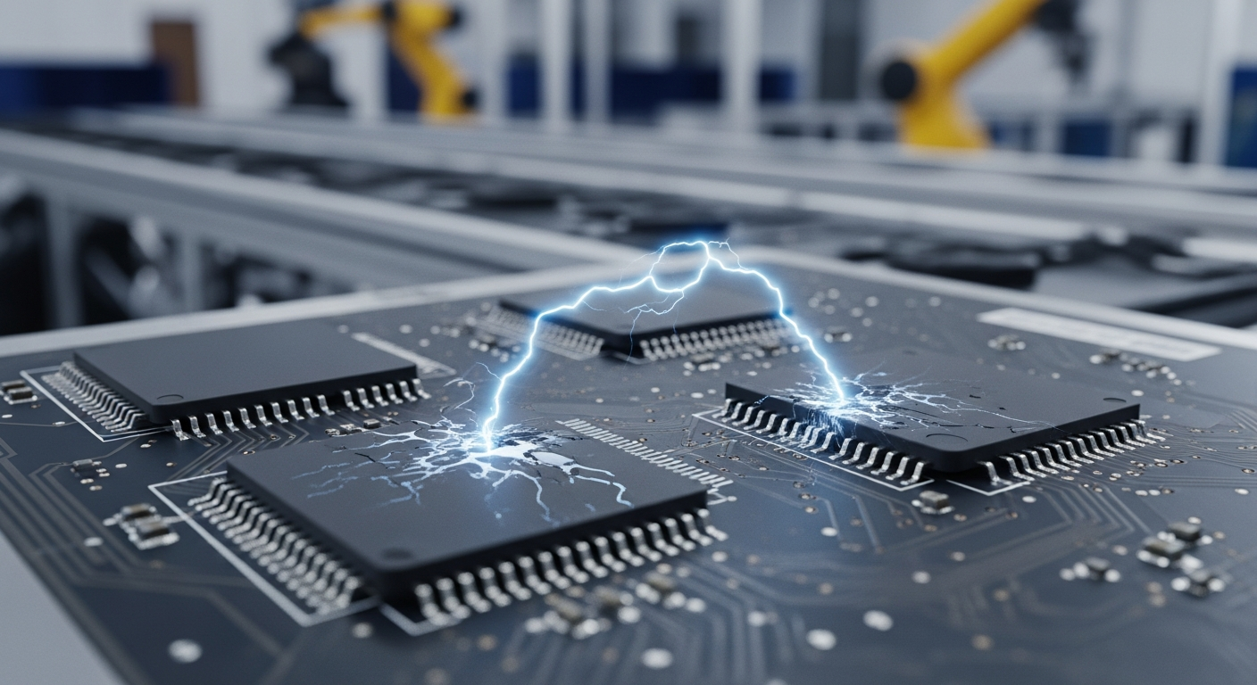
Latent Damage, Early-Life Failures, and Hard-to-Debug Issues
A component may pass AOI or ICT tests but fail under thermal load, vibration, or field use. ESD-damaged ICs show unstable behavior, communication errors, or random resets. Even tiny ESD sparks can corrupt memory or damage analog front-ends.
Engineering-driven factories perform incoming inspections, identify moisture-sensitive or ESD-sensitive components, and handle them with full ESD protocols. With coordinated SMT, DIP, and testing workflows, long-term stability is protected from early production onwards.
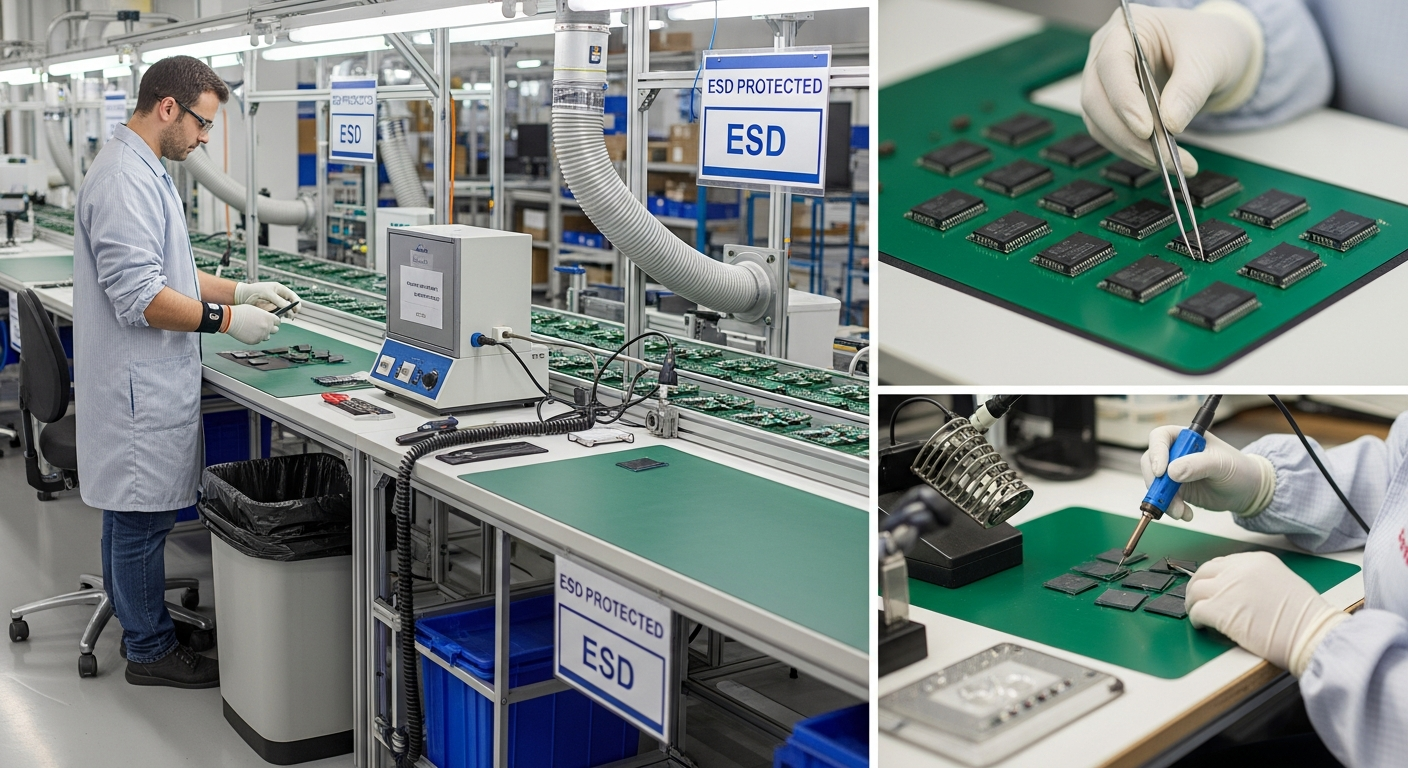
How do manufacturers maintain ESD-safe material flow?
Poor packaging or storage practices reintroduce ESD risks even after assembly.
Manufacturers use anti-static packaging, humidity controls, and proper storage to ensure safe handling.
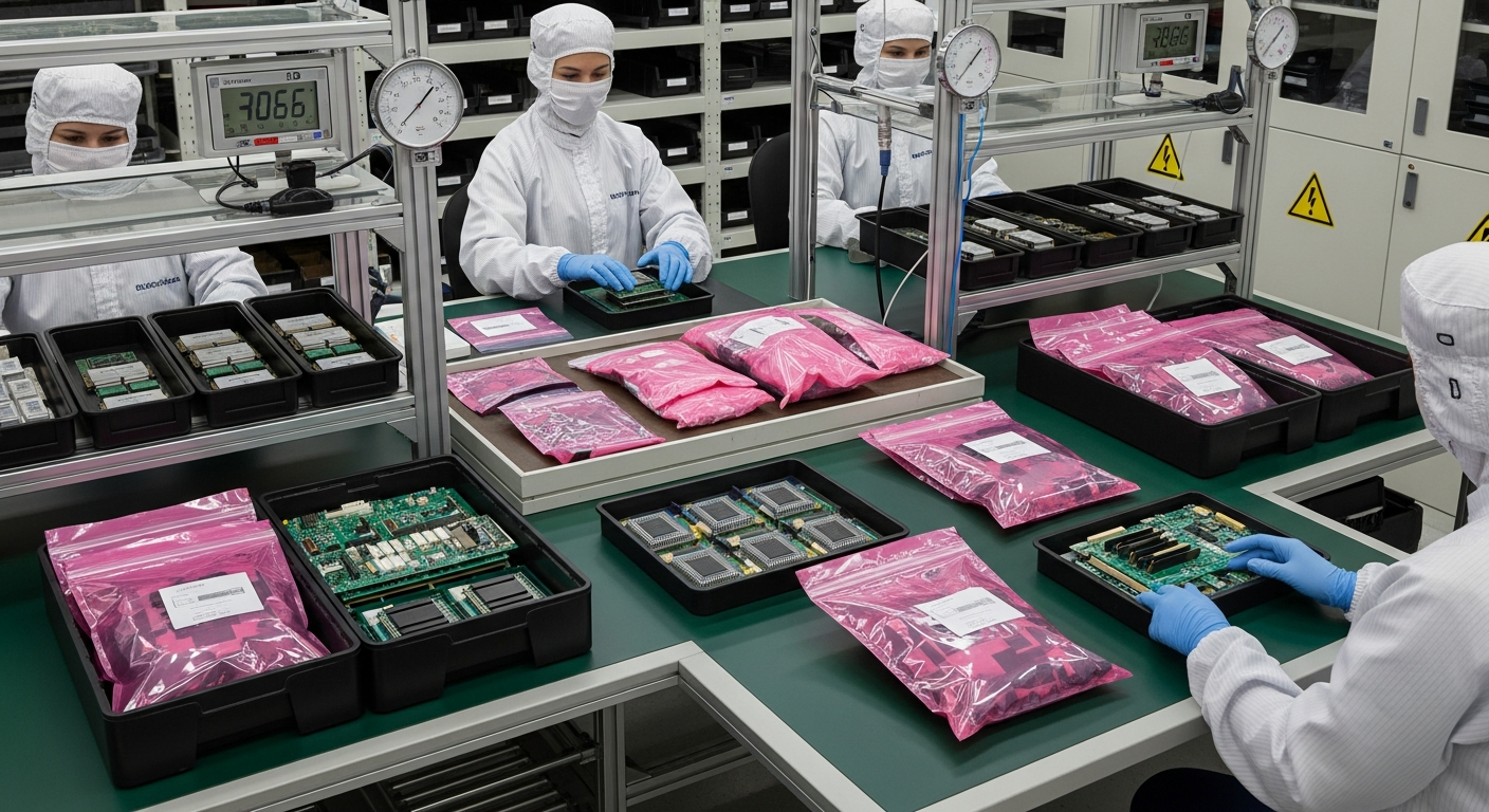
Controlled Packaging, Labeling, and Storage Conditions
Components are stored in anti-static bags, reels, or trays. Finished PCB assemblies are packed in ESD-safe foam and shielding bags. Labels identify sensitivity levels and handling instructions. Controlled humidity levels reduce charge build-up.
Integrated manufacturing partners track materials through ESD-safe zones from incoming materials to final shipment. This prevents recharging and protects products throughout the entire supply chain.
Conclusion
Electrostatic discharge (ESD) is a critical concern in electronics manufacturing, capable of damaging sensitive components and creating hidden reliability issues. Effective ESD control depends on grounded environments, certified materials, trained personnel, and consistent processes. When supported by engineering-driven PCB fabrication, SMT/DIP assembly, BOM management, and complete testing workflows, ESD protection becomes predictable and robust. This ensures higher product reliability, lower field failures, and smoother scaling from prototypes to global mass production.
