
Behind every modern electronic device lies an invisible structure controlling power, logic, and data with absolute precision.
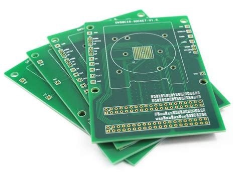
Printed circuit boards (PCBs) serve as the essential framework for connecting components and enabling seamless electronic functionality across countless devices.
From smartphones and laptops to life-saving medical instruments, these engineered boards are the reason our technology works reliably and efficiently. But what exactly happens beneath those layered surfaces? How do they channel power, manage signals, and ensure everything operates as one cohesive system? Let’s explore what makes PCBs the heartbeat of modern electronics.
The Foundation of Modern Electronics
At its core, a PCB is more than just a physical frame—it is a multilayered platform where electrical signals are precisely routed. A standard board is made from FR-4, a fire-retardant fiberglass composite known for excellent mechanical strength and insulation. On top of this base, copper layers are laminated, etched, and patterned to form the board’s conductive pathways.
These pathways, or traces, are like the roads in a micro-city. They carry electrical current between components and enable the board to perform logical, analog, and power management tasks. Every trace is calculated in terms of width, thickness, and distance to prevent signal interference, manage heat dissipation, and meet impedance requirements.
The layout is engineered using CAD tools that simulate trace performance, thermal distribution, and electromagnetic compatibility. This precision is essential for high-frequency and mixed-signal applications such as 5G base stations or medical imaging devices.
The Anatomy of a Circuit Board
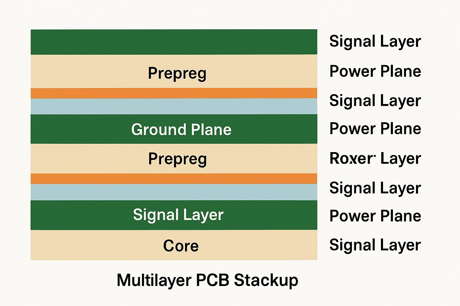
A modern circuit board consists of several layers stacked together to maximize functionality while minimizing size. Typical multilayer PCBs may contain:
- Signal layers for routing data
- Power planes for voltage supply
- Ground planes for electromagnetic shielding
- Prepreg and core dielectric materials for insulation
Advanced boards often include controlled impedance traces, blind/buried vias, and differential pairs to handle high-speed signals. These features enable complex systems like GPUs and communication modules to operate with extreme precision.
Every element in a PCB, from vias to copper pours, is driven by strict design-for-manufacturing (DFM) rules to ensure compatibility with fabrication and assembly processes.
Types of Printed Circuit Boards
Single-Sided PCBs
These are the simplest form of PCB, with copper traces on only one side. Though limited in complexity, they are cost-efficient and ideal for basic electronics like toys, LED circuits, and power adapters.
Advantages:
- Lower manufacturing cost
- Simplified assembly process
- Minimal design time
Limitations:
- Limited routing space
- Poor scalability for complex circuits
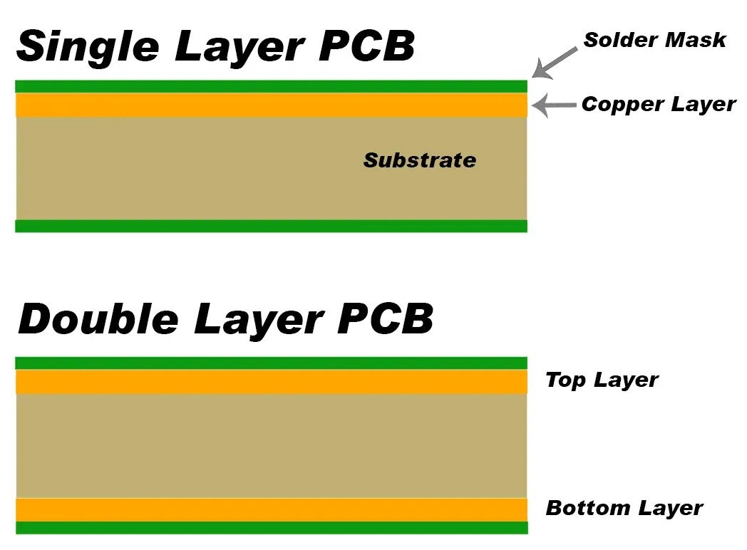
Double-Sided PCBs
Featuring copper layers on both sides, double-sided boards use plated through-holes (vias) to connect circuits between layers. These are widely used in mid-level electronics like consumer appliances and automotive modules.
Benefits:
- More component density
- Flexible trace routing
- Balanced performance vs cost
Multilayer PCBs
Multilayer boards start from four layers and can go up to 20+ layers in advanced applications. They’re standard in computing hardware, telecom systems, and high-frequency RF devices.
Use Cases:
- Servers, data centers
- Aerospace and defense
- Medical diagnostic equipment
Rigid, Flex, and Rigid-Flex PCBs
- Rigid boards offer mechanical strength and stability.
- Flexible PCBs can bend and twist, used in cameras, wearables, etc.
- Rigid-Flex PCBs combine both, often used in compact, mobile devices with 3D housing constraints.
Each type has unique implications for signal integrity, thermal management, and reliability testing.
The Role of Copper and Surface Finishes
Copper is the heartbeat of any PCB. It forms:
- Signal traces for high-speed communication
- Power distribution networks
- Ground reference planes
- Heat dissipation paths
Copper layer thickness ranges from 0.5 oz/ft² to 6 oz/ft², depending on current-carrying needs. High-power applications like EV chargers and industrial controls may use extra-thick copper.
To prevent oxidation and improve solderability, copper surfaces are treated with various surface finishes, such as:
| Finish Type | Benefit |
|---|---|
| HASL | Cost-effective, easy for manual soldering |
| ENIG | Excellent for fine-pitch components and longevity |
| Immersion Tin | Flat surface, suitable for SMT |
| Immersion Silver | Superior signal performance for RF circuits |
Surface finish choice directly affects assembly yield, storage life, and electrical performance, especially for fine-pitch and BGA components.
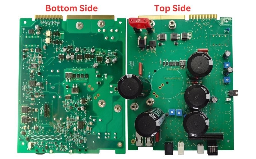
Key Components on a PCB
A PCB isn’t just copper and laminate—it’s a playground for both active and passive components. These devices determine the board’s purpose and performance.
Active Components
- Integrated Circuits (ICs): Include microcontrollers, processors, memory units. They handle data processing, control, and logic functions.
- Transistors: Enable switching and amplification. Essential for signal control and power management.
- Diodes: Direct current flow and protect circuits from voltage spikes.
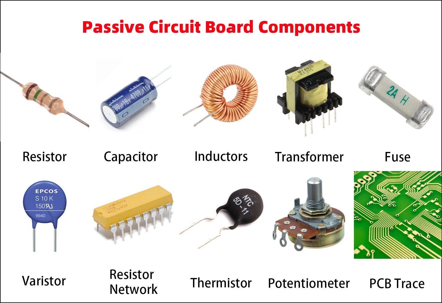
Passive Components
- Resistors: Regulate current and voltage levels.
- Capacitors: Store and release electrical energy, filter signals.
- Inductors: Store energy magnetically, used in filtering and power conversion.
Each component must be placed considering thermal load, signal timing, and EMI sensitivity—a task managed through meticulous PCB layout strategy.
From Design to Manufacturing
Design & Simulation
Everything starts with a schematic and netlist, then moves into layout. Tools like Altium Designer or KiCAD simulate electromagnetic behavior, thermal distribution, and manufacturability.
Fabrication Steps
- Lamination of substrate and copper foil
- Photoresist application and exposure
- Etching to form copper traces
- Drilling vias and plating through-holes
- Surface finish application
High-end PCBs may also undergo via-in-pad processing, microvia formation, and X-ray layer alignment.
Assembly Process
custompcba uses both Surface Mount Technology (SMT) and Through-Hole Technology (THT). SMT is dominant due to its speed and density advantages.
- Stencil printing of solder paste
- Pick-and-place of components using automated machines
- Reflow soldering under nitrogen atmosphere
- Inspection and quality control via AOI, X-ray, and functional testing
For rugged applications, conformal coating and thermal aging are added for long-term reliability.
Applications Across Industries
The versatility of PCBs extends to:
- Medical: ECG monitors, infusion pumps
- Aerospace: Satellite communication, radar systems
- Consumer electronics: Smartphones, TVs, smart speakers
- Automotive: ADAS, infotainment, battery management
- Industrial: Robotics, motor drives, PLCs
custompcba provides tailored solutions across all these sectors, offering both prototype and volume production with full traceability and compliance with IPC standards.
Conclusion
Printed circuit boards are the unseen heroes of our digital age. They organize, connect, and enable every function in a device, no matter how simple or sophisticated. From the fiberglass base to high-frequency copper traces and precision-mounted components, every detail counts.
Understanding how PCBs work isn’t just about knowing the layers—it’s about appreciating the engineering that brings hardware to life. With innovation in materials, manufacturing, and miniaturization, the future of circuit board design will only become more powerful and compact.
If you’re designing your next project or need a reliable partner for PCB production, custompcba is here to support your development from concept to creation.
