
Testing a PCB means verifying that it is electrically correct, mechanically stable, and functionally reliable before it is used or shipped. Proper PCB testing combines visual checks, electrical measurements, and functional validation to detect defects early and prevent long-term failures.
PCB testing is not a single step. It is a layered process that starts with simple inspection and ends with real operating verification.
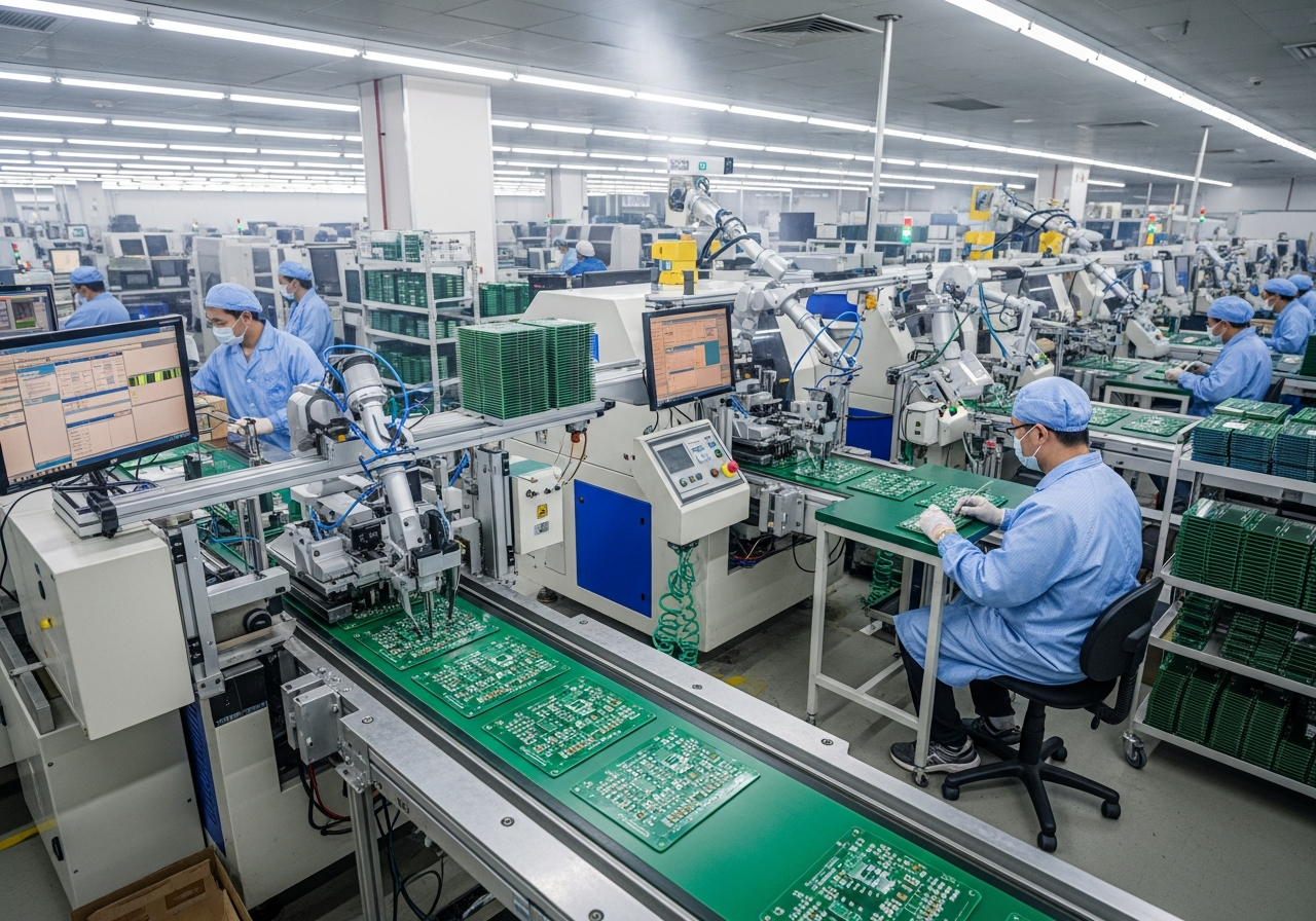
In professional manufacturing, PCB testing is designed to find problems as early as possible, when they are easiest and cheapest to fix.
What Is the First Step in PCB Testing?
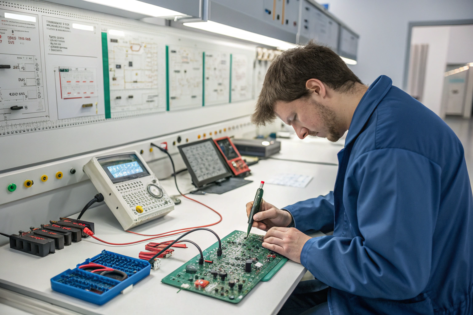
Every PCB test starts with visual inspection.
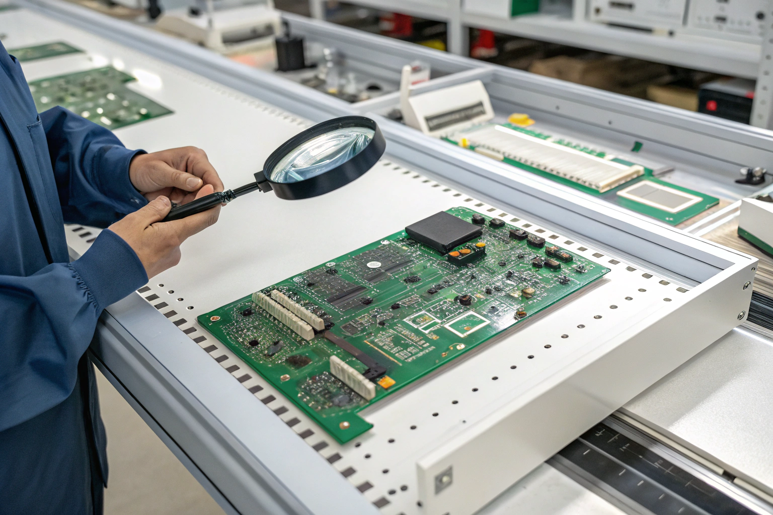
Many defects can be seen before power is applied.
Visual inspection checks for obvious assembly and material issues, including:
- Missing or misaligned components
- Solder bridges or solder splashes
- Cold or insufficient solder joints
- Lifted pads or damaged traces
- Burn marks or contamination
Magnification is strongly recommended. Small cracks, poor wetting, and hairline shorts are often invisible to the naked eye.
In factory workshops, microscopes and Automated Optical Inspection systems are used to ensure consistency. Catching visible defects early prevents powering a faulty board, which could cause further damage.
Visual inspection sets the foundation for all later testing stages.
How to Perform Basic Electrical Testing on a PCB?
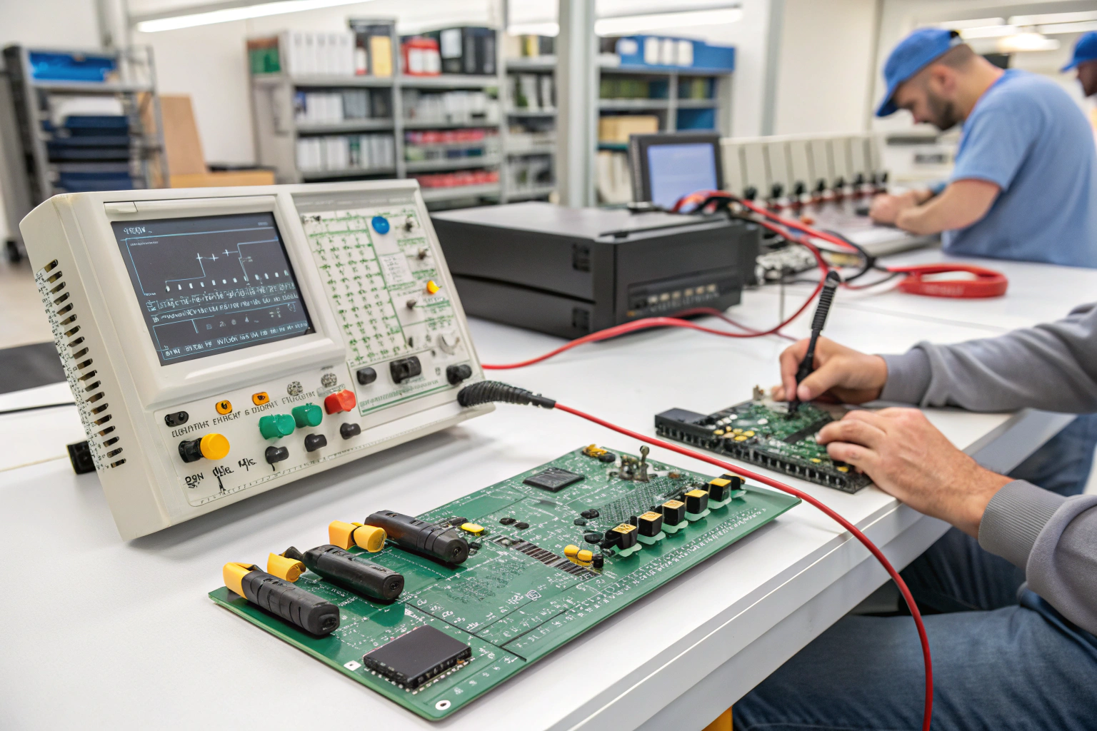
Electrical testing confirms that connections are correct.

It is done before full power-up.
Basic electrical tests include:
- Continuity testing
- Short-circuit detection
- Open-circuit verification
A multimeter is commonly used to check whether traces connect where intended and remain isolated where required. Power rails are checked for shorts to ground before any voltage is applied.
In manufacturing, this step prevents catastrophic failures. Applying power to a board with a shorted rail can destroy components instantly.
For more complex boards, fixture-based continuity testing or In-Circuit Testing is used to automate this step and reduce human error.
How to Safely Power On a PCB for the First Time?
Power-up testing must be controlled.
Uncontrolled power causes damage.
Before applying power:
- Verify correct input voltage
- Confirm polarity
- Use a current-limited power supply
During initial power-up, current draw is monitored closely. Abnormally high current indicates shorts or incorrect component placement. Power should be removed immediately if this occurs.
Key checks during power-up include:
- Stable voltage levels
- No excessive heating
- No smoke, smell, or noise
In professional environments, power-up is often done through test fixtures with built-in protection. This reduces risk and improves repeatability.
A safe first power-up protects both the PCB and the testing equipment.
How Functional Testing Confirms PCB Performance?
Functional testing proves that the PCB works.
It verifies real operating behavior.
Functional testing checks whether the PCB performs its intended tasks. This may include:
- Signal output verification
- Communication interface testing
- Sensor input response
- Load operation and control logic
Test conditions should match real usage as closely as possible. This includes voltage range, temperature, and operating load.
In factory production, functional test stations are customized for each product. Test software automates measurements and logs results for traceability.
A PCB that passes functional testing is not just assembled correctly. It is proven to work.
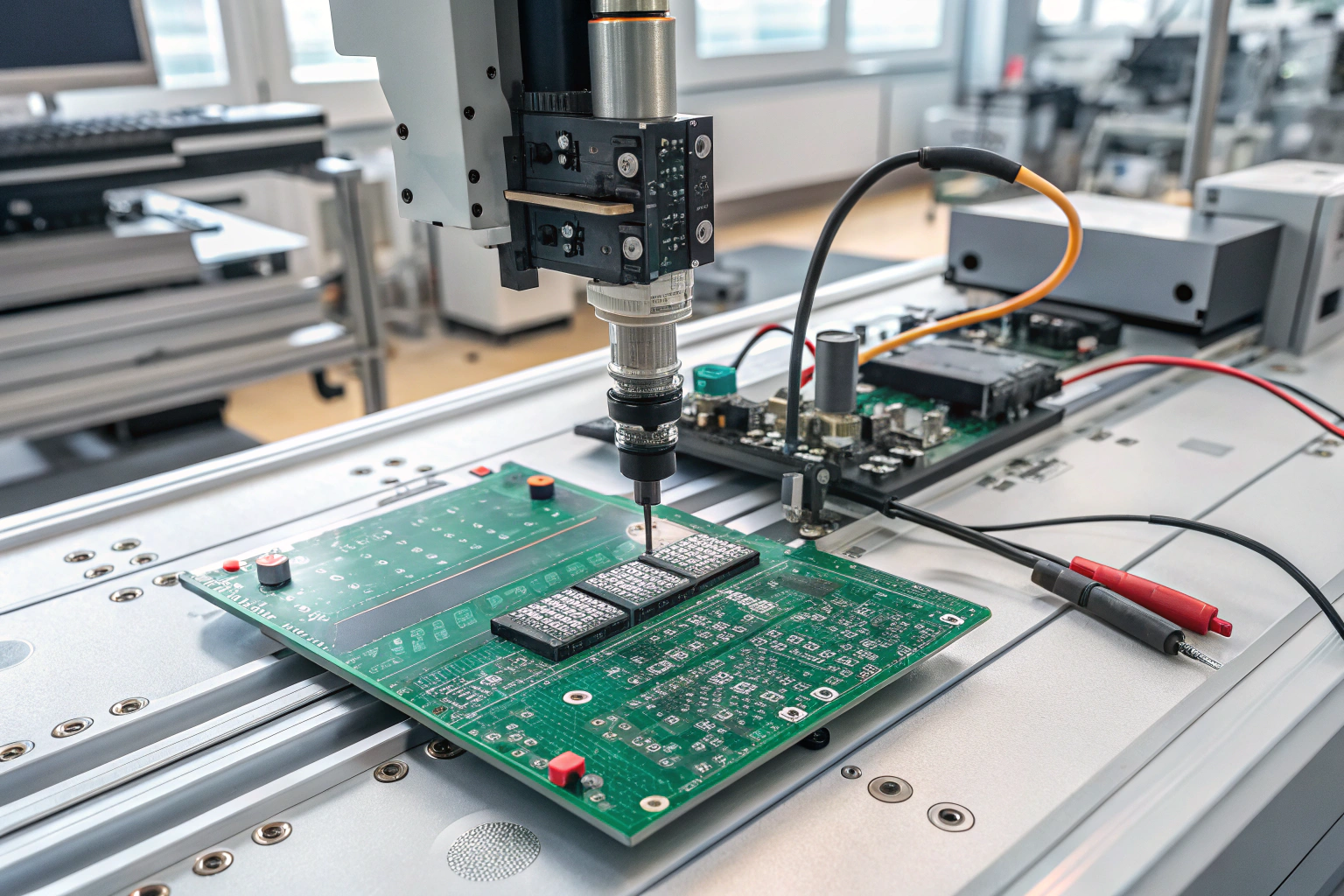
How In-Circuit Testing Improves PCB Test Coverage?
In-circuit testing isolates individual components.
It finds hidden electrical faults.
In-circuit testing uses probes or test points to measure components directly on the PCB. It checks:
- Resistor and capacitor values
- Diode polarity
- IC pin connectivity
- Solder joint integrity
This method identifies defects that functional testing may miss, such as incorrect component values or marginal solder joints.
In manufacturing, ICT is especially valuable for medium to high volume production. It increases fault detection rate and reduces troubleshooting time.
Designing sufficient test points into the PCB layout greatly improves test effectiveness.
How Advanced Testing Detects Hidden PCB Defects?
Some defects are invisible and intermittent.
Advanced tools reveal them.
Advanced PCB testing methods include:
- X-ray inspection for BGAs and hidden joints
- Thermal imaging to detect hot spots
- Boundary scan for complex digital circuits
- Stress testing under temperature cycling
X-ray inspection reveals voids, bridges, and misalignment under components that cannot be visually inspected.
Thermal cameras highlight abnormal heat patterns that indicate shorts or overloaded components.
These methods are common in professional workshops for high-density or high-reliability boards.
How Environmental and Stress Testing Validate Reliability?
A working PCB can still fail early.
Stress testing exposes weakness.
Environmental testing checks how a PCB behaves under:
- Heat and cold
- Humidity
- Vibration
- Extended operation
Thermal cycling accelerates solder joint fatigue. Burn-in testing runs the board continuously to reveal early-life failures.
In manufacturing, these tests are applied selectively based on product requirements. High-reliability products undergo stricter validation.
Stress testing does not guarantee infinite life, but it reduces unexpected field failures.
How Factory Testing Is Structured for PCB Production?
Testing is integrated, not isolated.
Each stage builds confidence.
In professional production lines, PCB testing follows a sequence:
- Visual inspection after assembly
- Electrical safety checks
- In-circuit testing
- Functional testing
- Final inspection and documentation
Test results are recorded and linked to each board. Failures trigger analysis and corrective action.
This structured approach ensures consistency across batches and prevents defective boards from moving downstream.
Testing is not a cost burden. It is a risk control system.
Conclusion
Testing a PCB requires a step-by-step approach that starts with visual inspection and progresses through electrical checks, controlled power-up, and functional validation. Advanced methods such as in-circuit testing, X-ray inspection, and stress testing reveal hidden defects and long-term reliability risks. In professional manufacturing, PCB testing is integrated into every production stage to ensure consistency and traceability. A properly tested PCB is not only functional at the moment of test, but stable, predictable, and ready for real-world operation over its full service life.
