
Multilayer PCBs are a fundamental part of modern electronic products. As circuits become more complex, faster, and smaller, single or double layer boards can no longer meet electrical and manufacturing requirements. Multilayer PCBs solve these challenges by organizing electrical functions across multiple internal copper layers.
Multilayer PCBs work by stacking and laminating multiple copper layers inside insulating materials, allowing signals, power, and ground to be separated, controlled, and interconnected through plated vias.
This structure improves electrical performance, mechanical stability, and production consistency.
The following sections explain how multilayer PCBs function from structural, electrical, and manufacturing perspectives.
How Is a Multilayer PCB Structured?
Layered structure is the core principle.
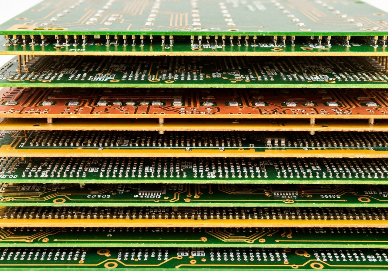
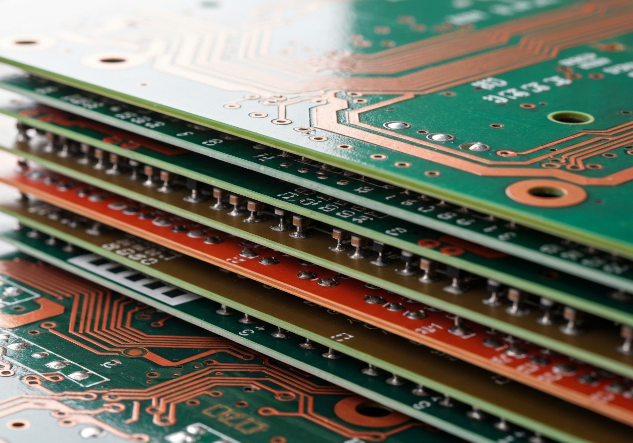
A multilayer PCB consists of alternating copper layers and dielectric materials that are permanently bonded into a single rigid board.
A typical multilayer PCB includes:
- Outer layers for component mounting and signal routing
- Internal signal layers for dense routing
- Dedicated power planes
- Dedicated ground planes
Each layer is assigned a specific role. By separating functions across layers, electrical behavior becomes more predictable and easier to control compared to surface-only routing. From a manufacturing standpoint, symmetric layer structures also improve mechanical balance and reduce warpage during thermal processing.
How Do Signals Flow Inside a Multilayer PCB?
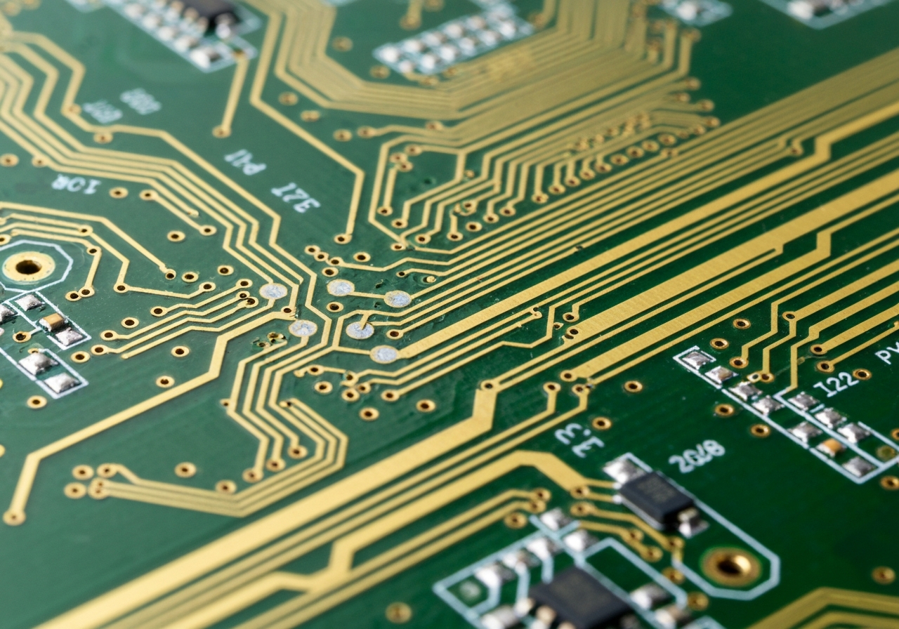
Signals travel in controlled paths.
In multilayer PCBs, electrical signals run along copper traces on specific layers. When a signal needs to move between layers, it travels vertically through plated vias.
Routing signals on inner layers adjacent to solid ground planes provides clear return paths and controlled impedance. This reduces signal reflection, crosstalk, and timing variation.
Compared with single or double layer boards, multilayer signal routing shortens trace length and improves signal integrity, especially for high-speed digital and communication circuits.
How Do Power and Ground Layers Work?
Power stability is built into the structure.
One of the key advantages of multilayer PCBs is the use of continuous power and ground planes.
These planes:
- Distribute current evenly across the board
- Lower power distribution impedance
- Reduce voltage drop
- Improve decoupling capacitor effectiveness
A solid ground plane also provides a stable reference for signal return currents. This greatly reduces electrical noise and random functional instability during operation and testing.
How Are Layers Electrically Connected?
Vias create vertical connections.
Vias are plated holes that electrically connect copper layers inside the PCB.
Common via types include:
- Through-hole vias connecting all layers
- Blind vias connecting outer to inner layers
- Buried vias connecting internal layers only
These structures allow three-dimensional routing inside the board. However, via quality is critical. In manufacturing, drilling accuracy, desmear quality, and copper plating thickness are tightly controlled to ensure long-term reliability under thermal cycling.
How Does Lamination Enable Multilayer PCBs to Work?
Lamination turns layers into one solid structure.
During manufacturing, inner layers, prepregs, and copper foils are stacked in a defined sequence and pressed together under heat and pressure.
The resin in the prepreg flows and cures, bonding all layers into a single rigid board. Proper lamination ensures:
- Accurate layer alignment
- Strong interlayer adhesion
- Controlled board thickness
- Minimal warpage
Without stable lamination control, multilayer PCBs would suffer from delamination, misregistration, and early failure during assembly or long-term use.
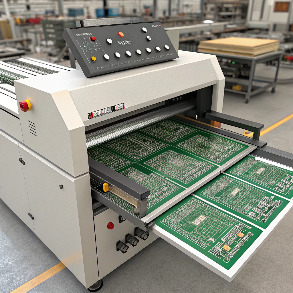
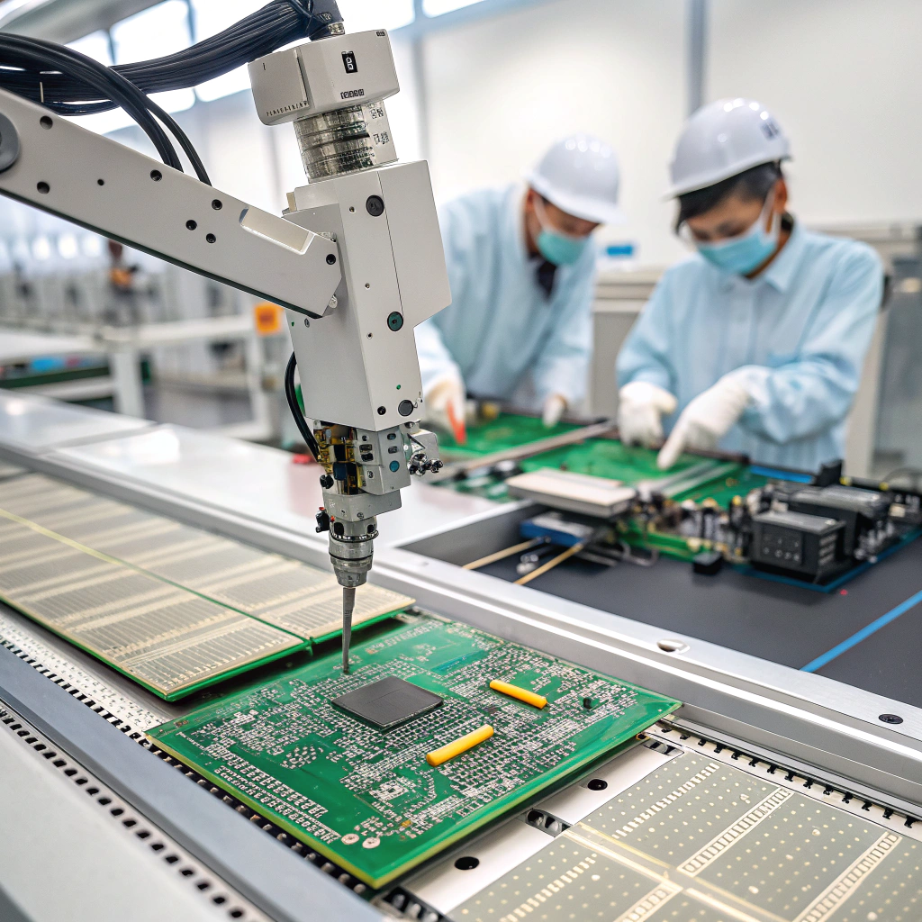
How Do Factory Processes Ensure Multilayer PCB Performance?
Manufacturing discipline ensures consistency.

Multilayer PCB performance depends heavily on factory process control.
Key workshop controls include:
- Inner-layer AOI inspection before lamination
- Precise stack-up and alignment control
- Stable lamination temperature and pressure
- Controlled drilling and desmear processes
- Via copper plating thickness monitoring
- Electrical testing and final inspection
These controls ensure that internal layers function as designed and remain stable across production batches.
How Do Multilayer PCBs Improve Assembly and Reliability?
Structure supports stable assembly.
Balanced multilayer stack-ups reduce internal stress and improve rigidity.
In SMT workshops, multilayer PCBs show:
- Less warpage during reflow soldering
- Better coplanarity for fine-pitch components
- More consistent solder joint quality
- Higher AOI and functional test pass rates
This stability improves yield and reduces rework during mass production.
Conclusion
Multilayer PCBs work by distributing electrical functions across multiple internal copper layers that are permanently bonded into a single structure. Signals travel through controlled paths, power and ground planes stabilize electrical behavior, and vias connect layers vertically to enable complex routing.
From a manufacturing perspective, multilayer PCBs rely on precise lamination, drilling, plating, and inspection processes to ensure internal integrity. When these processes are well controlled, multilayer PCBs deliver high signal integrity, stable power distribution, reliable assembly performance, and long-term durability. This combination of electrical performance and manufacturing consistency makes multilayer PCBs a foundational technology for modern electronic products requiring scalability, reliability, and predictable quality.
