
Printed Circuit Board (PCB) damage is one of the most critical risks in electronic manufacturing. A damaged PCB can cause functional failure, unstable performance, or hidden reliability issues that only appear after long-term use. In professional manufacturing environments, PCB damage is closely analyzed because it often reflects deeper problems in design control, workshop handling, or process execution.
PCB damage rarely happens without a reason. It is usually the result of mechanical stress, thermal exposure, electrical misuse, or improper process control. Understanding how a PCB gets damaged requires a full view of materials, assembly processes, factory conditions, and post-assembly handling. The following sections explain the most common damage mechanisms from a manufacturing perspective.
How Can Mechanical Stress Damage a PCB?
Mechanical stress is one of the most direct causes of PCB damage. Even when electrical design is correct, physical forces can permanently compromise board integrity.
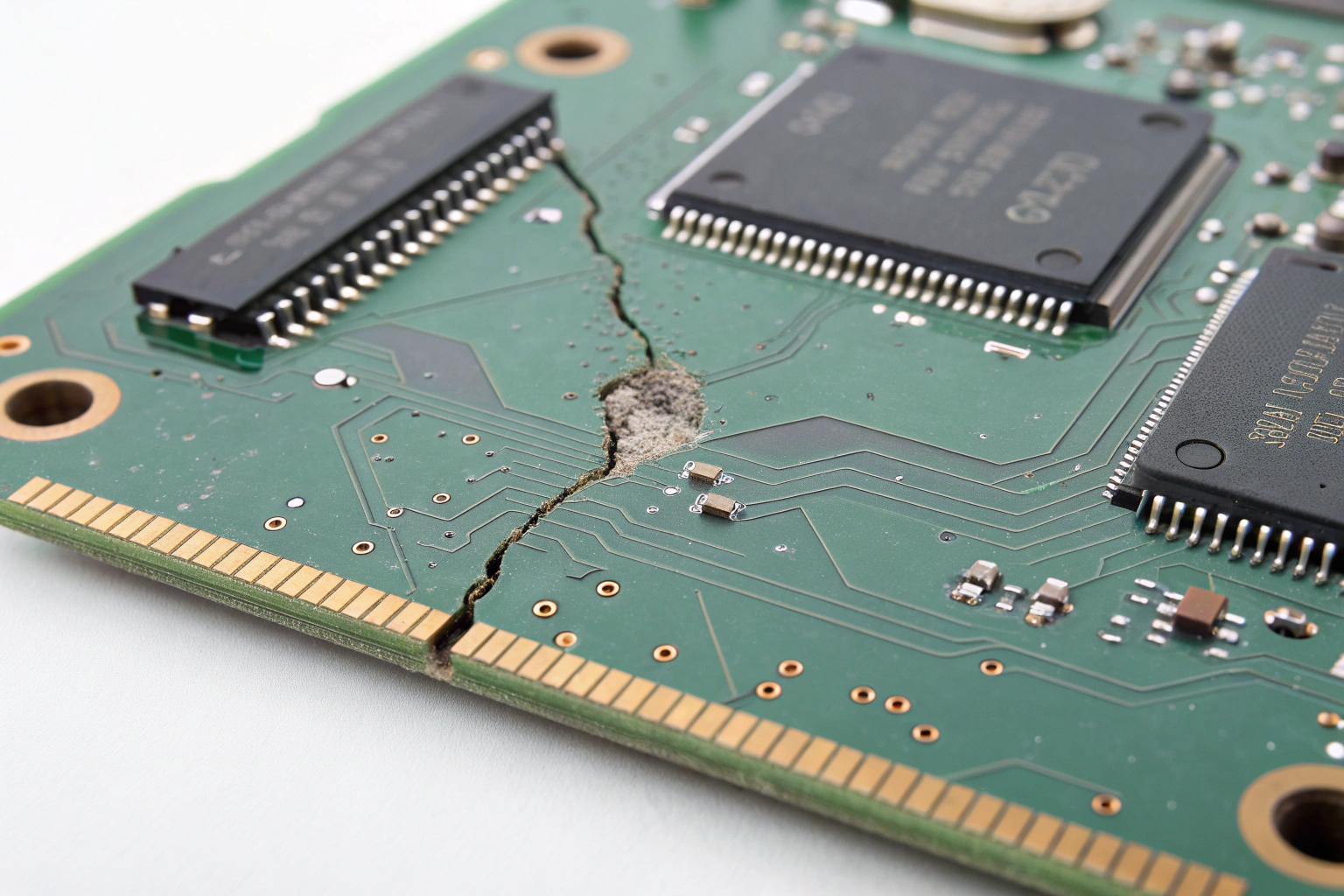
Common mechanical damage includes:
- Cracked PCB substrates
- Lifted or broken copper traces
- Damaged solder joints due to bending
- Broken connectors or component leads
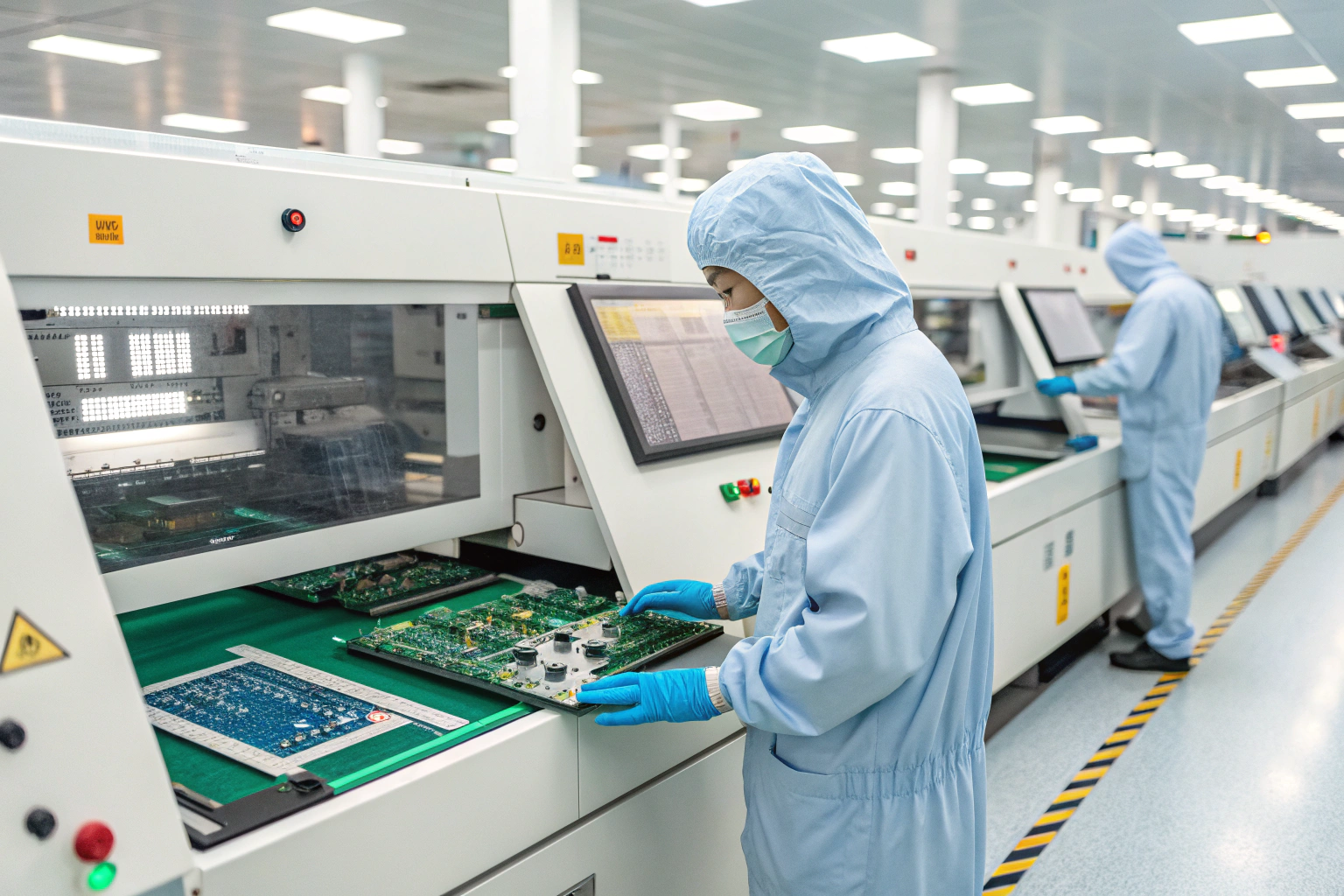
In factory workshops, mechanical stress often occurs during depaneling, manual handling, or fixture installation. Improper depaneling methods, such as uncontrolled snapping instead of router or laser separation, can introduce micro-cracks that are invisible during inspection.
During assembly and testing, boards must be supported evenly to avoid flexing. Professional manufacturing lines use dedicated carriers and fixtures to control board movement. Mechanical damage is especially critical for thin PCBs and high-density layouts, where even small deformation can lead to long-term reliability failures.
How Does Thermal Exposure Cause PCB Damage?
Thermal stress is another major factor that damages PCBs during manufacturing and operation. PCBs are designed to withstand specific temperature ranges, but excessive or uneven heat can exceed material limits.
Typical thermal damage includes:
- Delamination of PCB layers
- Pad lifting from excessive rework
- Component cracking due to thermal shock
- Solder joint fatigue and brittleness
In SMT workshops, thermal exposure mainly comes from reflow soldering and rework processes. Incorrect reflow profiles, such as excessive peak temperature or rapid cooling, can weaken solder joints and damage PCB materials.
Rework stations require precise temperature control. Repeated heating of the same area significantly increases damage risk. Manufacturing engineers monitor reflow curves and limit rework cycles to protect PCB structure. Proper thermal management during assembly is essential for maintaining board strength and reliability.
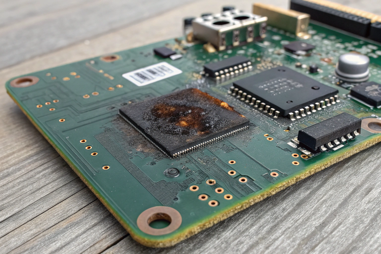
How Can Electrical Issues Physically Damage a PCB?
Electrical misuse or design errors can also lead to physical PCB damage, not just functional failure.
Electrical damage often includes:
- Burnt traces caused by overcurrent
- Carbonization of PCB material
- Exploded or cracked components
- Short circuits leading to localized overheating
In production environments, electrical damage is commonly detected during power-on testing or functional testing. Incorrect power supply connection, reversed polarity, or missing protection circuits can quickly destroy sensitive areas of the PCB.
Manufacturing testing stations use current-limited power supplies to reduce damage risk. Electrical damage is often irreversible, resulting in scrap boards. Such failures highlight the importance of thorough electrical design review, controlled testing procedures, and clear polarity markings during assembly.
How Do Assembly and Process Errors Damage PCBs?
Assembly process errors are a frequent source of PCB damage, especially when process discipline is weak.
Process-related damage includes:
- Solder bridges causing overheating
- Excessive solder leading to component stress
- Improper cleaning causing corrosion
- Misaligned components stressing pads
In SMT workshops, solder paste printing accuracy, placement precision, and reflow stability directly affect PCB health. Poor stencil design or unstable paste viscosity can create solder defects that later damage the board during operation.
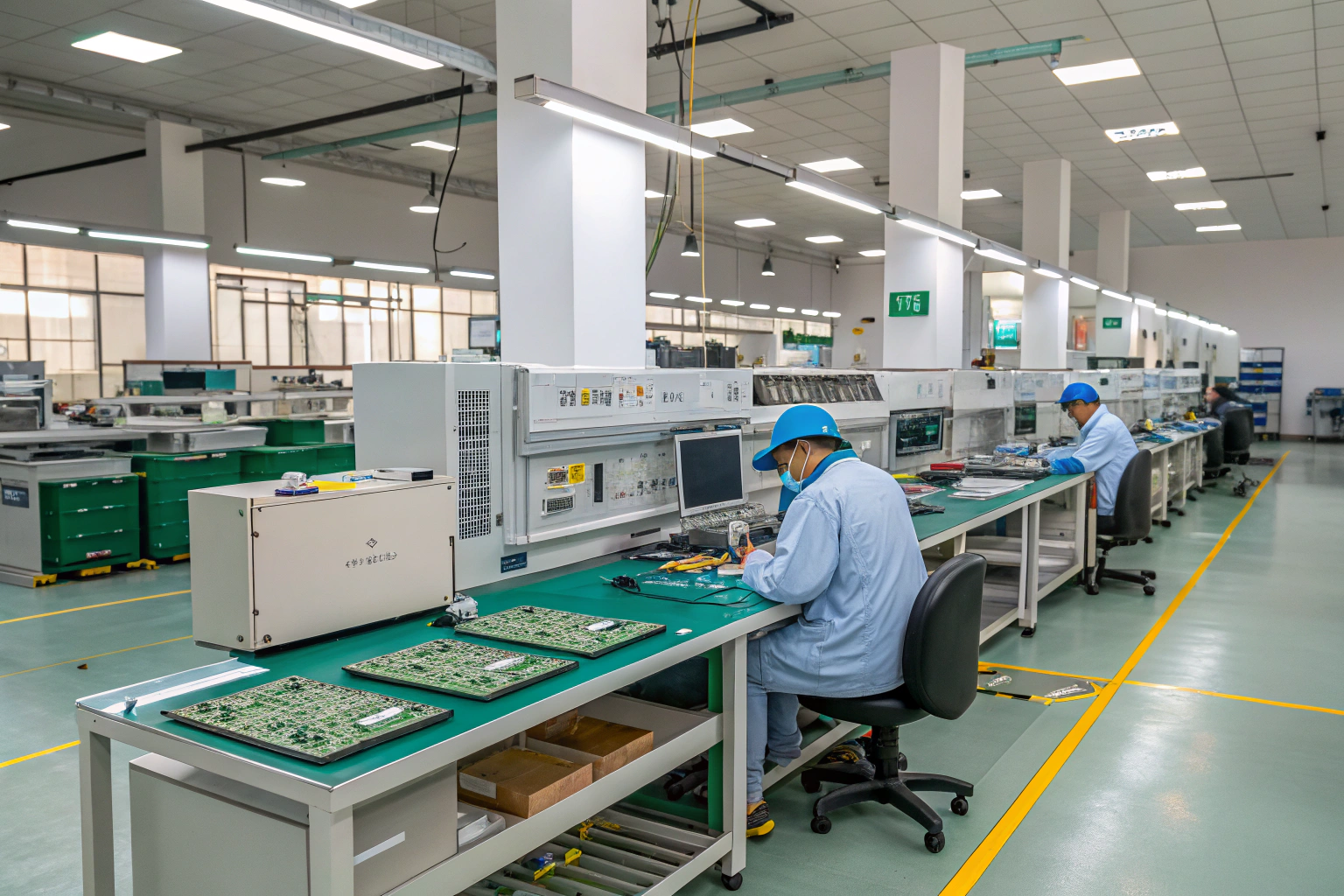
Manual handling during assembly or inspection can also introduce damage if ESD protection and handling rules are not strictly followed. Professional factories rely on standardized work instructions, operator training, and automated inspection systems to minimize assembly-induced damage.
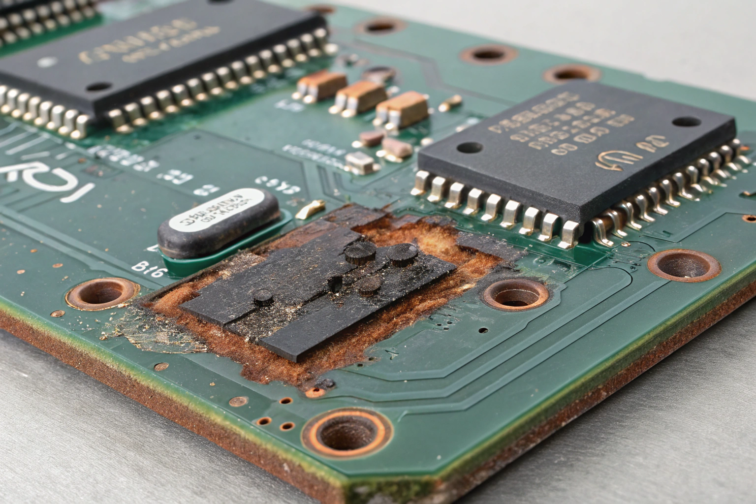
How Do Environmental Factors Lead to PCB Damage?
Environmental exposure can damage PCBs during storage, transport, or operation if not properly controlled.
Common environmental damage includes:
- Corrosion from moisture or condensation
- Oxidation of exposed copper
- Mold growth in high-humidity conditions
- Insulation breakdown due to contamination
In manufacturing facilities, humidity control and proper storage are critical. Moisture-sensitive components and bare PCBs are stored in dry cabinets or moisture barrier packaging. Failure to control moisture can result in delamination or soldering defects during reflow.
Environmental damage may not cause immediate failure but often leads to reduced lifespan. Manufacturing quality systems include incoming material inspection and controlled storage conditions to prevent such hidden risks.
How Does Poor Process Control Increase PCB Damage Risk?
Weak process control amplifies all other damage mechanisms. Without stable processes, even good designs and materials can fail.
Key process weaknesses include:
- Inconsistent machine calibration
- Lack of ESD control
- Inadequate inspection coverage
- Poor traceability and documentation
In professional manufacturing environments, every PCB passes through defined checkpoints. AOI, electrical testing, and functional testing act as safety nets to detect early damage. Process data is reviewed regularly to identify trends before they escalate into widespread failures.
Facilities with integrated SMT lines, rework stations, and testing capability can respond faster to process deviations. Strong process control reduces damage risk and improves long-term product stability.
Conclusion
PCB damage is the result of combined mechanical, thermal, electrical, environmental, and process-related factors. It rarely comes from a single mistake. In manufacturing environments, damaged PCBs are treated as signals that reveal weaknesses in design control, workshop handling, or process execution. By strengthening process discipline, controlling workshop conditions, and applying structured inspection and testing, PCB damage can be significantly reduced. A mature manufacturing system does not simply repair damaged boards but continuously improves processes to protect PCB integrity from assembly through final use.
