
PCB production is a multi-stage industrial process that converts design data into a finished circuit board ready for assembly. In standard manufacturing practice, the complete PCB production flow can be summarized into seven core steps, each supported by dedicated workshops, equipment, and process controls.
Although PCB complexity varies by layer count and application, these seven steps form the backbone of professional PCB manufacturing and determine final electrical performance, reliability, and yield.
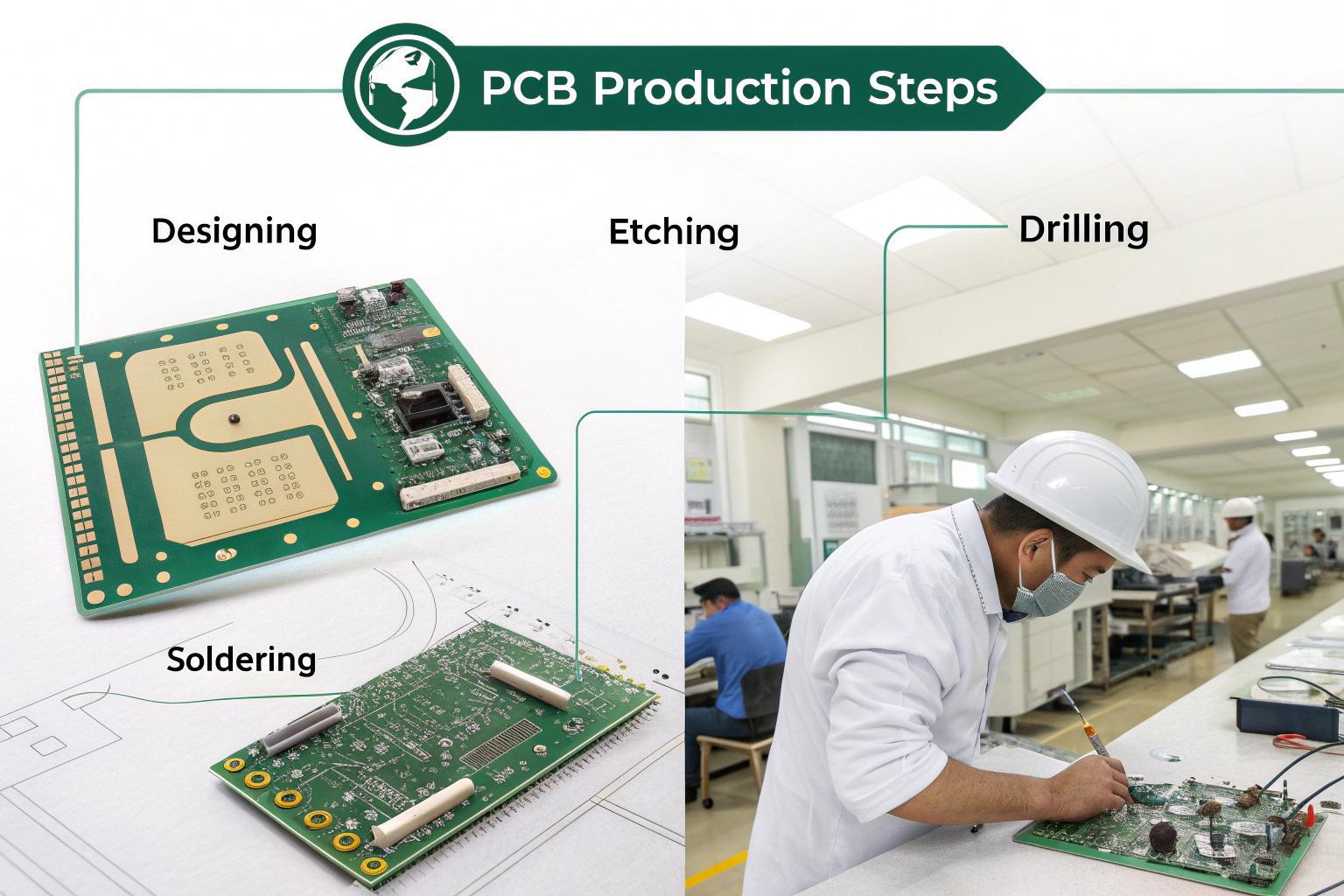
Design data preparation and engineering review
PCB production begins with digital design data. This includes Gerber files, drill files, stack-up details, and technical notes. Engineering teams review these files to confirm manufacturability.
Key checks include trace width and spacing, hole sizes, annular rings, solder mask clearance, and impedance requirements. Panelization methods are also defined at this stage to improve material usage and production efficiency.
From a factory perspective, this step connects design intent with process capability. Early detection of risks reduces rework and prevents production delays. A structured engineering review ensures the following steps can proceed smoothly and consistently.
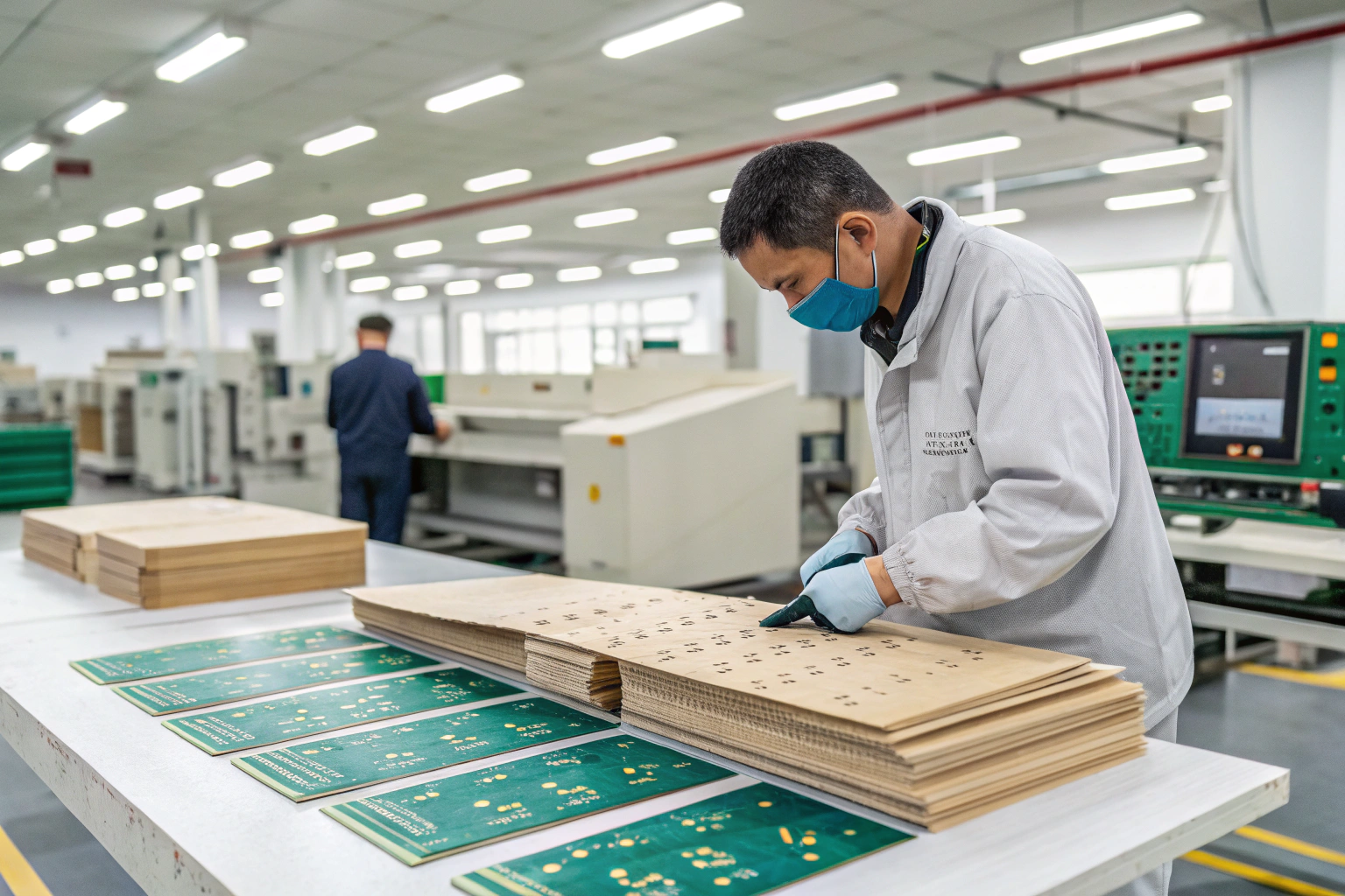
Raw material selection and cutting
Once design data is approved, raw materials are prepared. Copper-clad laminates, prepregs, and copper foils are selected according to layer count, electrical requirements, and mechanical strength.
Materials are inspected for thickness tolerance, surface quality, and storage condition. Laminates are then cut into production panels based on the defined panel size.
Material control inside the factory is critical. Stable material properties ensure consistent lamination results and predictable electrical behavior, especially for multilayer boards.
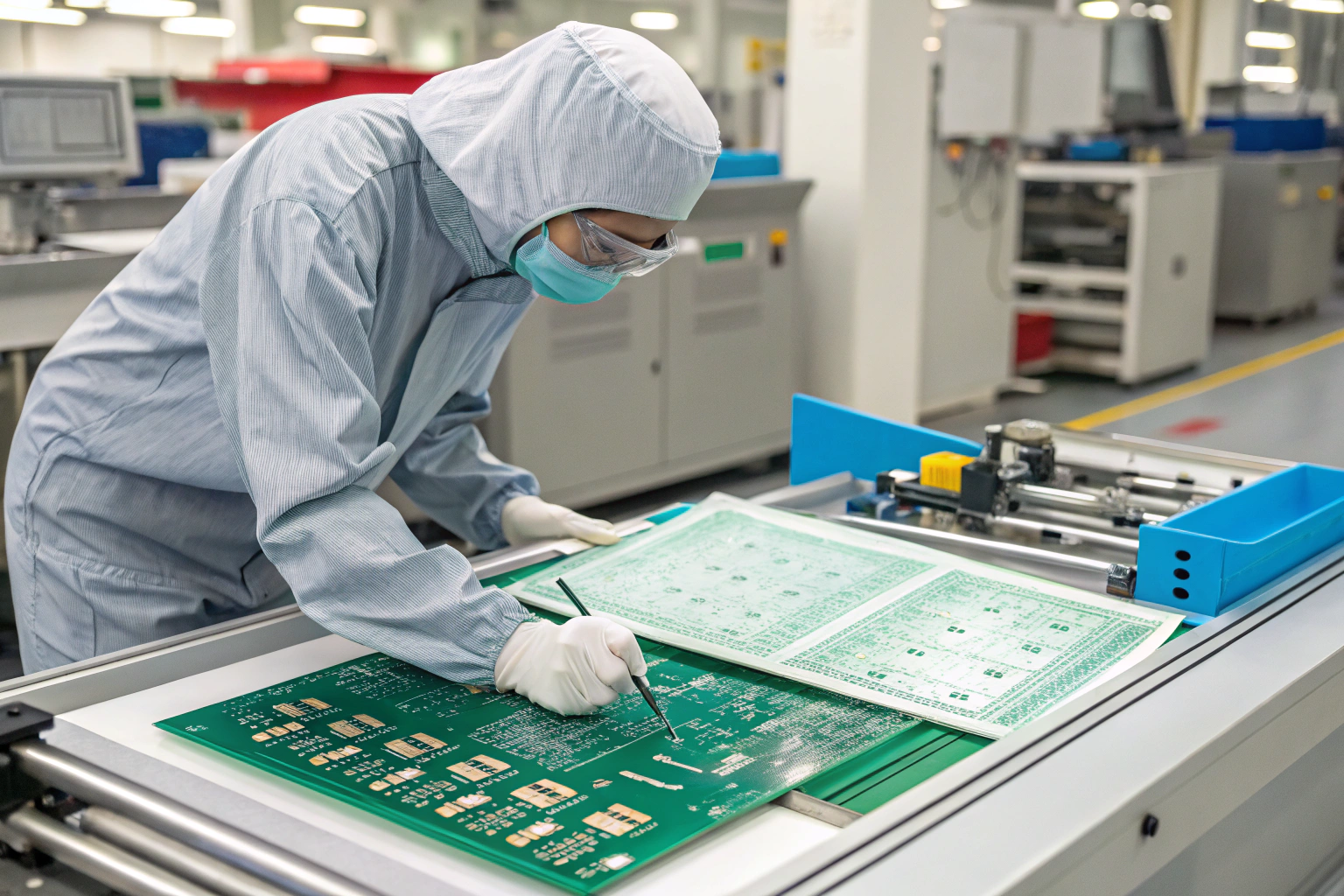
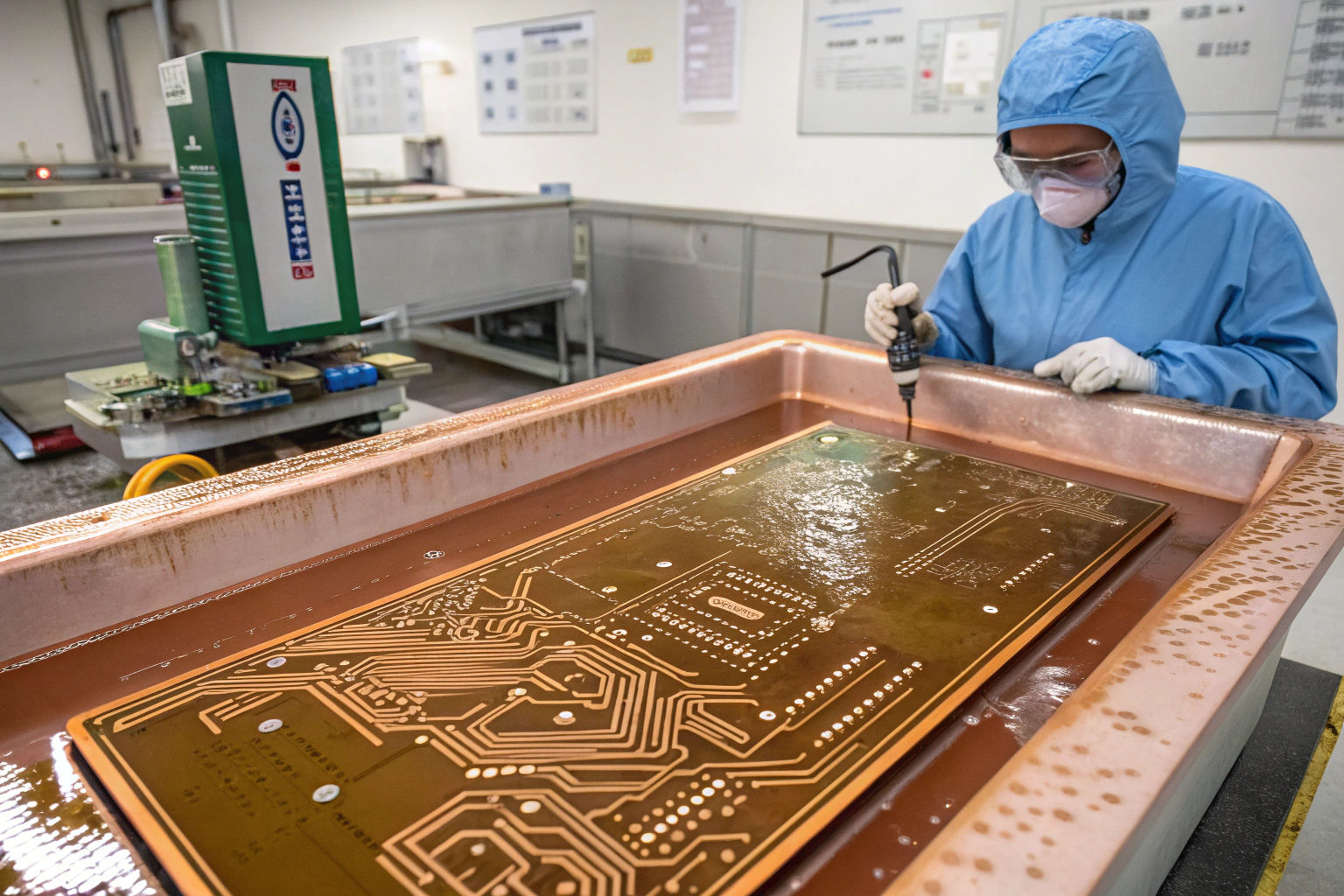
Inner layer imaging and etching
For multilayer PCBs, inner layers are processed first.
Copper surfaces are cleaned and coated with photoresist. Circuit patterns are transferred using laser or UV exposure. After development, unwanted copper is removed through chemical etching.
After etching, automated optical inspection checks trace width, spacing, and defects. Approved inner layers form the electrical core of the PCB. Precision at this step directly affects signal integrity and long-term reliability.
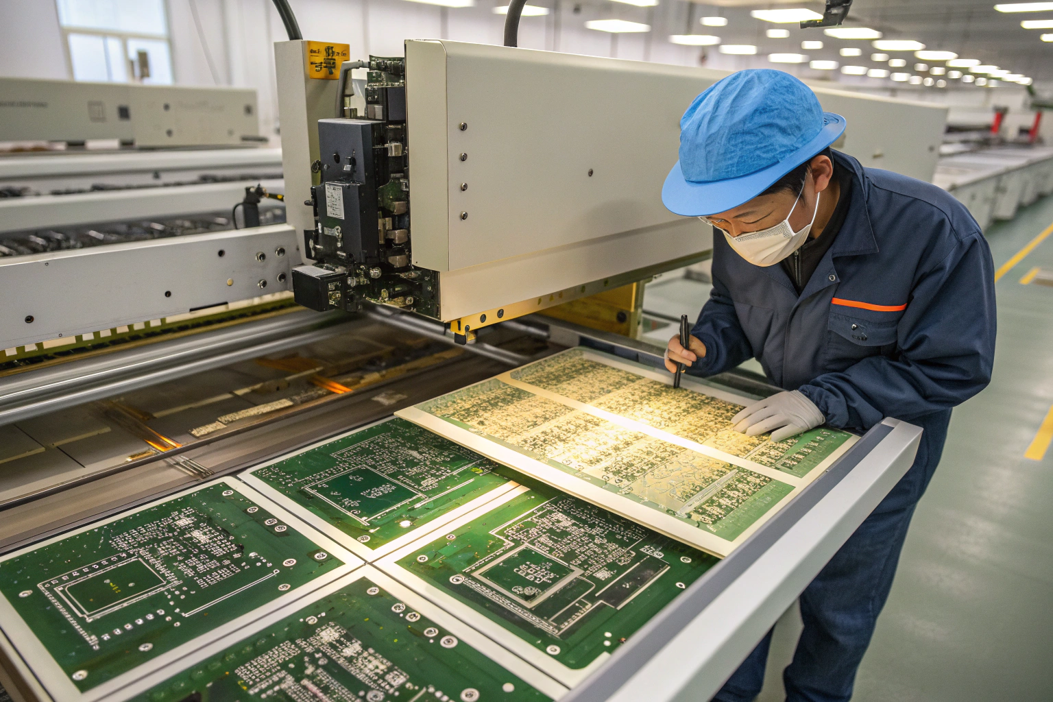
Lamination and drilling
Inner layers are stacked with prepreg and copper foil according to the stack-up design. The stack is pressed under controlled heat and pressure to form a solid multilayer structure.

After lamination, CNC drilling machines create vias and through holes. Drilling accuracy determines plating quality and interlayer connection reliability. Tool wear, speed, and alignment are closely monitored in the drilling workshop.
Plating and outer layer circuit formation
Drilled holes are metallized using electroless copper plating, followed by electroplating to build sufficient copper thickness. This creates reliable electrical connections between layers.
Outer layer circuits are then imaged and etched in a process similar to inner layers. Copper thickness uniformity and adhesion are key quality indicators at this stage.
Solder mask, surface finish, and silkscreen
Protective and functional coatings are added after circuit formation.

Solder mask is applied to insulate copper traces and prevent solder bridging during assembly. Surface finishes such as ENIG, HASL, or OSP are applied to exposed pads to improve solderability.
Silkscreen printing adds reference designators, polarity marks, and identification text. Clear marking improves assembly efficiency and inspection accuracy.
Electrical testing, final inspection, and packaging
Before shipment, finished PCBs undergo electrical testing to verify continuity and isolation. Visual inspection checks board outline, surface quality, and labeling.
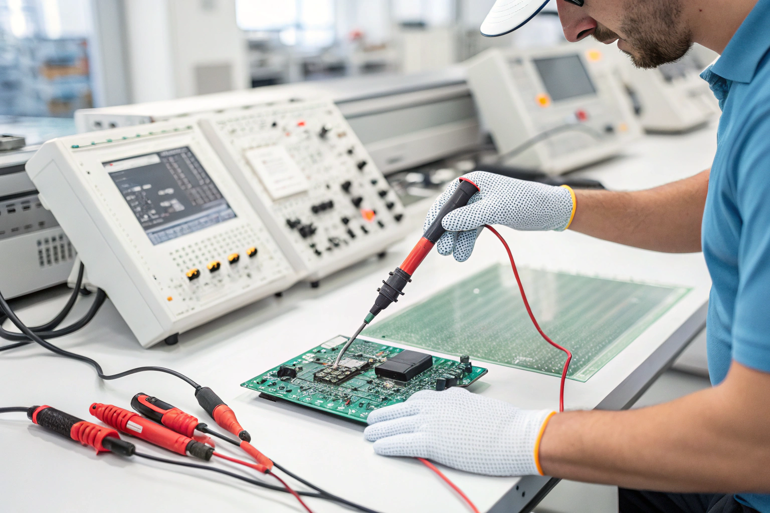
Quality teams review inspection records and test results. Approved boards are cleaned and packed using moisture-proof and anti-static materials to protect them during storage and transportation.
Conclusion
PCB production typically involves seven essential steps, from engineering review and material preparation to lamination, plating, and final testing. Each step is carried out in specialized factory workshops and supported by strict process control.
When these steps are executed under a disciplined manufacturing system, the result is a PCB with stable electrical performance, strong mechanical structure, and high assembly compatibility. A clear, standardized production flow not only improves yield and consistency but also ensures that the PCB can reliably support complex electronic systems throughout their entire service life.
