
Printed Circuit Board (PCB) faults are one of the most common causes of electronic product failure. These issues may appear during prototyping, small-batch production, or even after mass manufacturing. If not handled correctly, PCB faults can lead to unstable performance, shipment delays, and high rework costs.
Fixing a PCB fault is not a single action. It is a structured engineering process that combines fault analysis, testing, process control, and manufacturing experience. This article explains how PCB faults are identified and fixed in a professional manufacturing environment, with a strong focus on production workshops, process control, and quality assurance.
A systematic approach to PCB fault repair not only solves current problems but also prevents repeated failures in future production runs. The following sections outline six key stages commonly used in professional PCB assembly factories.
What Are the Most Common PCB Fault Types?
PCB faults usually fall into several repeatable categories, each linked to design, materials, or manufacturing processes.
Common PCB fault types include:
- Soldering defects such as cold joints, solder bridges, and insufficient solder
- Component-related issues including wrong parts, reversed polarity, or damaged ICs
- PCB fabrication defects such as open circuits, short circuits, and delamination
- Assembly alignment problems caused by inaccurate placement or warped boards
- Functional failures due to signal integrity, power instability, or EMI issues
From a manufacturing perspective, most PCB faults are not random. They usually point to weaknesses in DFM review, soldering profiles, material selection, or operator control. Identifying the fault category is the first step toward an effective fix.
In a factory workshop, fault statistics are tracked by defect type and process stage. This data-driven method helps engineering teams quickly focus on the real root cause instead of relying on guesswork.
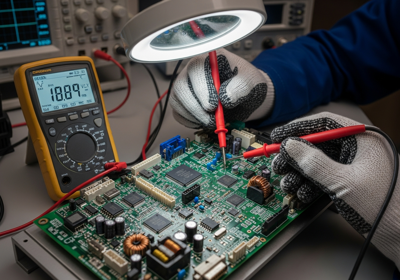
How Is a PCB Fault Diagnosed Step by Step?
Accurate diagnosis is the foundation of successful PCB fault repair. Skipping this step often leads to repeated failures or hidden reliability risks.
A standard diagnosis flow includes:
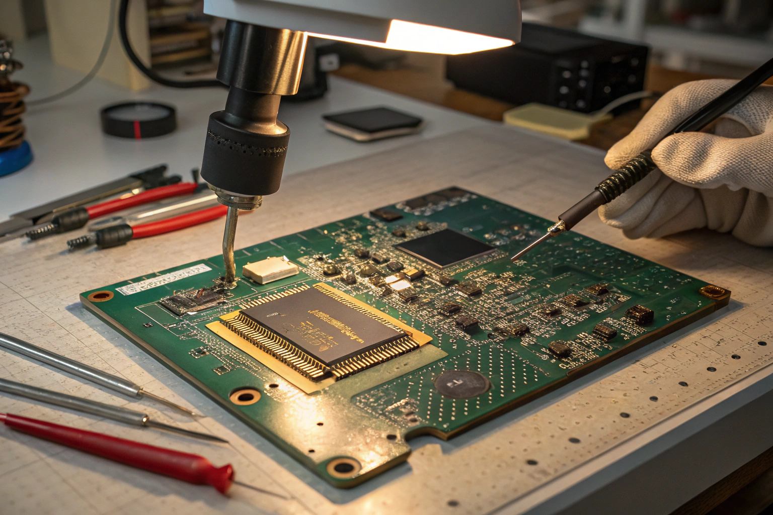
- Visual inspection under magnification
- Electrical testing using multimeters and test fixtures
- Functional testing under real operating conditions
- Signal analysis using oscilloscopes or logic analyzers
- Thermal inspection for overheating components
In a professional SMT workshop, automated tools such as AOI and X-ray inspection are widely used. AOI identifies solder defects and placement errors, while X-ray inspection is essential for BGA and QFN packages where solder joints are hidden.
Engineering teams also review Gerber files, BOMs, and assembly drawings during diagnosis. Many faults originate from mismatched footprints, unclear polarity markings, or missing assembly notes. A structured diagnostic process ensures that both electrical and process-related issues are covered.
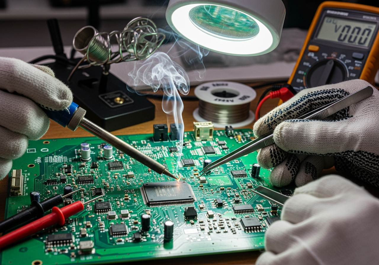
How Are Soldering-Related PCB Faults Fixed?
Soldering defects account for a large percentage of PCB faults, especially in high-density designs.
Typical soldering repairs include:
- Reflowing cold solder joints with controlled temperature
- Removing solder bridges using solder wick or hot air
- Replacing components damaged by overheating
- Reinforcing weak joints with proper flux and solder alloy
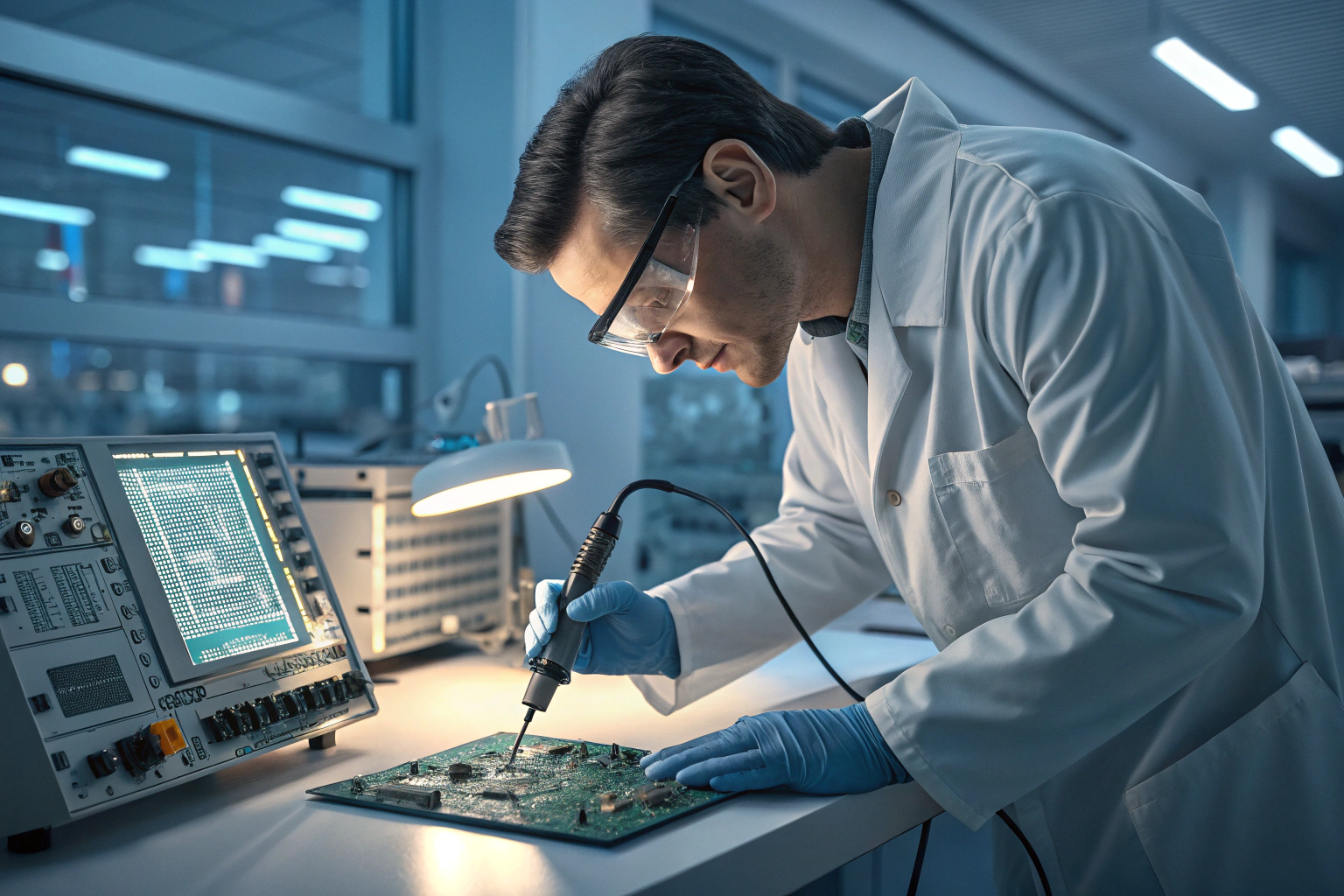
In a factory environment, soldering repair is performed in dedicated rework stations. These stations use ESD protection, temperature-controlled tools, and standardized rework procedures. Random manual fixes are avoided to reduce secondary damage.
Process engineers also review the original reflow profile after soldering faults are found. Incorrect soak time, peak temperature, or cooling rate often causes recurring defects. Adjusting the process prevents the same fault from appearing in the next production batch.
How Do Component and Material Issues Get Resolved?
Component-related faults are often more complex than soldering problems. These issues may involve incorrect part selection, counterfeit components, or material compatibility problems.
Resolution steps usually include:
- Verifying part numbers and specifications against the BOM
- Testing suspect components individually
- Replacing components with verified alternatives
- Reviewing storage and handling conditions
In professional workshops, components are stored under controlled humidity and temperature. Sensitive devices such as ICs and MOSFETs follow strict MSD handling rules. When faults occur, material traceability records help identify whether the issue is linked to a specific batch or supplier.
Engineering teams also evaluate component substitutions. If a part becomes unavailable or unstable, qualified alternatives are tested to ensure electrical and thermal compatibility. This approach reduces supply risks while maintaining product reliability.
How Does the Manufacturing Process Affect PCB Fault Repair?
Many PCB faults are symptoms of deeper process problems rather than isolated mistakes.
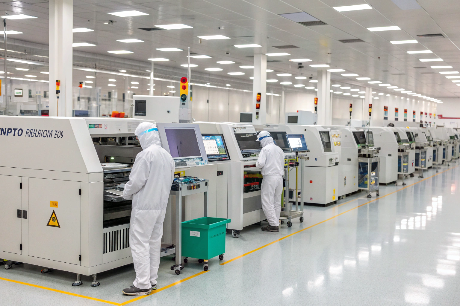
Key manufacturing factors include:
- Accuracy of SMT placement machines
- Stencil design and solder paste quality
- PCB panelization andFIDIAL alignment
- Operator training and process discipline
In modern SMT workshops, machines are regularly calibrated, and process parameters are logged for traceability. When a PCB fault is detected, engineers trace it back to a specific process step, machine, or shift.
Repair actions are often combined with process optimization. For example, repeated tombstoning issues may lead to stencil redesign, while frequent misalignment may require improved fiducial recognition. This closed-loop improvement system ensures that PCB fault repair strengthens overall manufacturing quality.
How Can Future PCB Faults Be Prevented?
Prevention is the most cost-effective form of PCB fault management. Fixing a single board is useful, but preventing thousands of failures is far more valuable.
Effective prevention measures include:
- Thorough DFM and DFA reviews before production
- Clear assembly drawings and polarity markings
- Pilot runs and first article inspections
- Consistent functional testing and reporting
- Continuous process audits and staff training
In a manufacturing setting, prevention is built into daily operations. Test data, defect reports, and repair records are reviewed regularly by engineering and quality teams. This information feeds back into design guidelines and process standards.
Factories with in-house SMT lines, testing capability, and engineering support can respond faster to issues and apply improvements without long communication delays. This integrated approach significantly reduces long-term failure rates.
Conclusion
Fixing a PCB fault is a structured engineering task, not a quick manual adjustment. It requires accurate diagnosis, controlled repair methods, and strong manufacturing discipline. When supported by a well-managed workshop, stable processes, and experienced engineering teams, PCB fault repair becomes an opportunity to improve product reliability and production efficiency. A mature repair and prevention system ensures consistent quality from prototype to full-scale production.
