
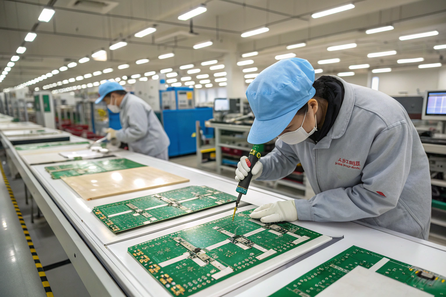
As electronic products become more complex and compact, multilayer PCBs have become a standard solution to meet higher requirements for routing density, signal integrity, and manufacturing reliability. Compared with single or double layer boards, multilayer PCBs require more controlled processes and stricter factory management.
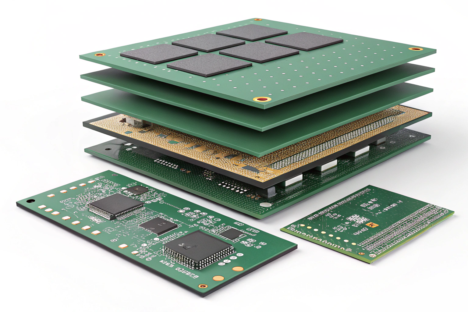
A multi layer PCB is made by fabricating inner circuit layers first, stacking them with prepreg and core materials, laminating them under heat and pressure, then completing drilling, plating, outer-layer processing, and inspection.
Each step is tightly connected and directly affects final quality.
The following sections explain how multilayer PCBs are manufactured step by step, with a focus on real factory workshop processes.
Inner Layer Circuit Fabrication
Inner layers form the foundation of a multilayer PCB.
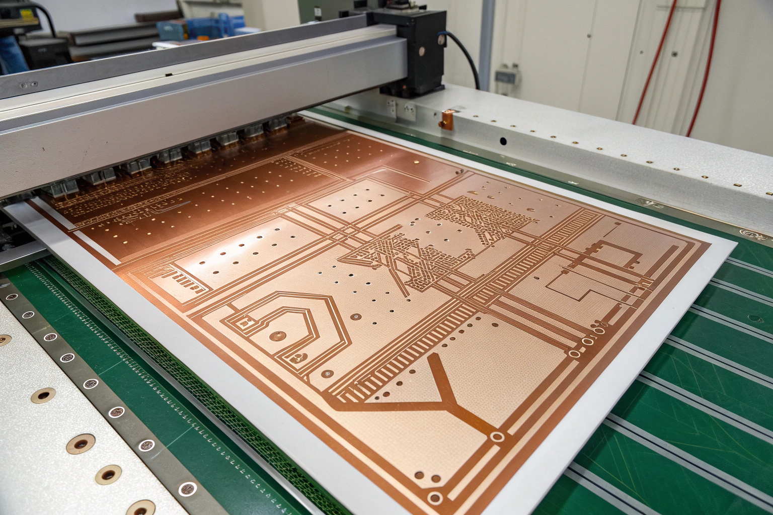
Manufacturing starts with copper-clad core materials. Each inner layer circuit is created by imaging and etching processes.
The typical workflow includes:
- Copper surface cleaning
- Dry film photoresist lamination
- UV exposure using circuit artwork
- Developing and chemical etching
- Photoresist stripping
After etching, inner layers undergo AOI inspection to detect shorts, opens, and line width deviations. This inspection is critical because inner-layer defects cannot be repaired once lamination is completed. Only qualified inner layers are released to the next stage.
Stack-Up Preparation and Lay-Up
Correct stack-up determines long-term reliability.
Before lamination, inner copper layers receive oxide or alternative surface treatment to improve bonding strength with resin materials.
The lay-up process stacks materials in a defined sequence:
- Inner copper layers
- Prepreg sheets
- Core materials
- Outer copper foils
Layer alignment accuracy is tightly controlled during this stage. Misalignment can reduce annular ring size, affect via reliability, and lead to electrical failures later in production or use.
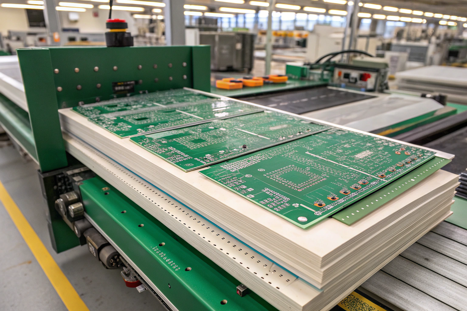
Lamination Pressing Process
Lamination turns multiple layers into one board.
The stacked panels are placed into a lamination press where heat and pressure cure the resin and bond all layers together.
Key lamination controls include:
- Temperature ramp and dwell time
- Pressure distribution
- Resin flow behavior
- Final board thickness and flatness
For higher layer counts or HDI structures, multiple lamination cycles may be required. Lamination quality directly affects warpage, delamination resistance, and long-term mechanical stability.
Drilling, Desmear, and Via Preparation
Vertical connections enable layer interconnection.
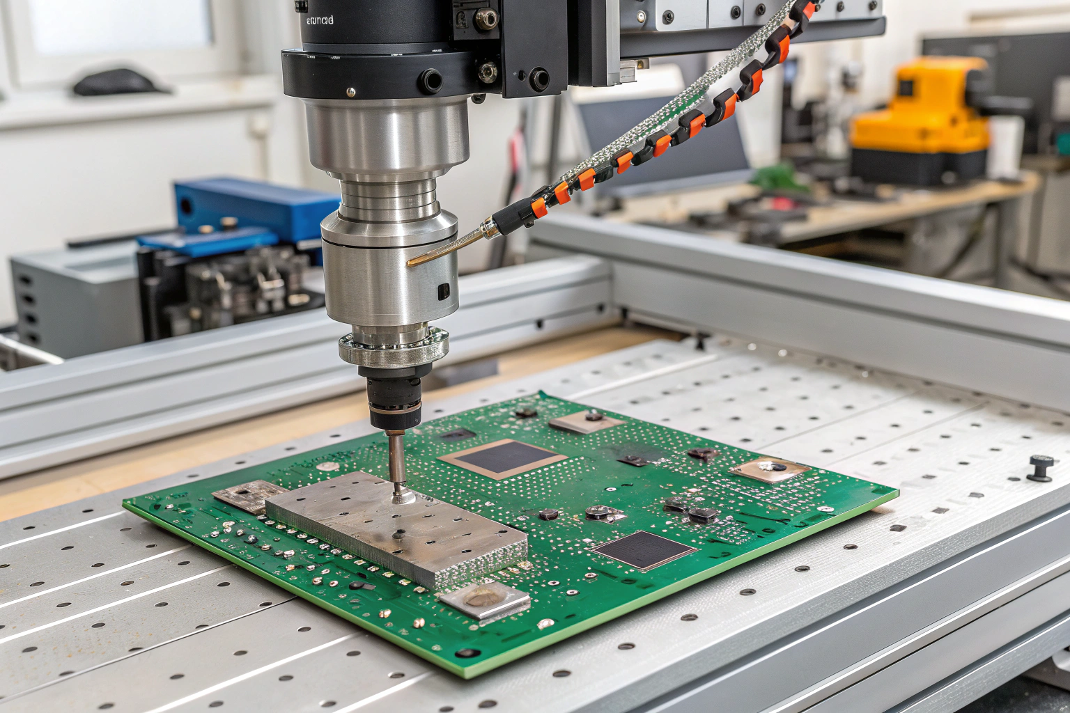
After lamination, holes are drilled to form vias and component holes.
Drilling methods include:
- Mechanical drilling for standard vias
- Laser drilling for microvias
Drilling leaves resin smear on hole walls, which must be removed through desmear processing. Clean hole walls are essential for strong copper adhesion during plating. Poor desmear is a common root cause of via failures in multilayer PCBs.
Copper Plating and Outer Layer Circuit Formation
Electrical connections are completed.
A thin copper layer is first deposited chemically, followed by electroplating to build copper thickness on hole walls and outer layers.
After plating, outer layers are imaged and etched to form final surface circuits. AOI inspection is performed again to verify trace width, spacing, and pad integrity. This step often represents a major yield control point in fine-line designs.
Solder Mask, Surface Finish, and Profiling
Protection and solderability are added.
Solder mask is applied and cured to protect copper traces and define solderable areas.
Common surface finishes include ENIG, lead-free HASL, and OSP. Finish selection affects solderability, shelf life, and assembly consistency.
Boards are then routed or V-scored to define the final outline. Outline accuracy is essential for enclosure fit and downstream assembly processes.
Factory Testing and Quality Control
Testing ensures internal layers work as designed.
Multilayer PCBs undergo electrical testing to verify continuity and isolation between all nets.
Factory quality control typically includes:
- Electrical test (flying probe or fixture)
- Visual inspection
- Dimensional and thickness measurement
- Process record traceability
For high-reliability designs, cross-section analysis may be used to verify internal layer alignment and plating thickness.
Conclusion
Making a multi layer PCB is a structured manufacturing process that builds electrical functionality layer by layer through controlled imaging, lamination, drilling, plating, and inspection. Each stage depends on the accuracy and stability of the previous one, making process discipline essential throughout production.
From a factory perspective, multilayer PCB manufacturing relies on standardized stack-ups, mature lamination processes, and rigorous quality control systems. When inner-layer accuracy, lamination stability, and via reliability are well controlled, multilayer PCBs deliver high signal integrity, stable assembly performance, and long-term reliability. This combination of electrical performance and manufacturing consistency makes multilayer PCBs a fundamental solution for modern electronic products requiring scalability and dependable quality.
