
The PCB manufacturing process is a structured industrial workflow that transforms design data into a reliable physical circuit board. It combines engineering control, material science, precision equipment, and standardized workshop operations to ensure electrical performance and long-term stability.
A professional PCB manufacturing process is not a single operation. It is a complete system that starts from design data preparation and ends with quality-approved boards ready for assembly. Each step affects yield, consistency, and downstream PCBA performance.
How does design data preparation start PCB manufacturing?
PCB manufacturing begins with digital design data. This includes Gerber files, drill files, stack-up information, and technical notes. These files define copper layers, trace width, spacing, hole sizes, and board outline.
Before production, engineering teams perform a manufacturability review. Trace spacing, annular ring size, solder mask clearance, and impedance requirements are checked against process capability.
This step connects design intent with factory reality. Designs that align with fabrication limits reduce rework and improve yield. Panelization methods are also defined at this stage to optimize material usage and production efficiency.
A controlled design review process ensures that potential risks are resolved before materials are committed, creating a stable foundation for all subsequent steps.
How are raw materials selected and prepared?
Material selection determines both electrical and mechanical performance of the PCB.
The most common base material is FR4, while high-frequency or high-temperature applications may require specialized laminates. Copper foil thickness, prepreg type, and core structure are chosen based on layer count and application requirements.
Incoming materials are inspected for thickness tolerance, surface cleanliness, and storage condition. Laminates and prepregs are stored under controlled temperature and humidity to prevent moisture absorption.
Stable material management inside the factory ensures consistency across batches. This consistency is critical for multilayer boards, where even small material variations can affect impedance and layer alignment.
How is inner layer imaging and etching performed?
For multilayer PCBs, inner layers are processed first.
Copper-clad laminates are cleaned and coated with photoresist. Imaging equipment transfers circuit patterns onto the photoresist using laser or UV exposure. After development, unwanted copper is removed through chemical etching.
Process control during etching is critical. Etching speed, chemical concentration, and temperature directly affect trace width accuracy. After etching, inner layers undergo optical inspection to verify line width, spacing, and defects.
High-quality inner layers ensure correct electrical paths and prevent latent failures after lamination. This step defines the core signal integrity of the PCB.
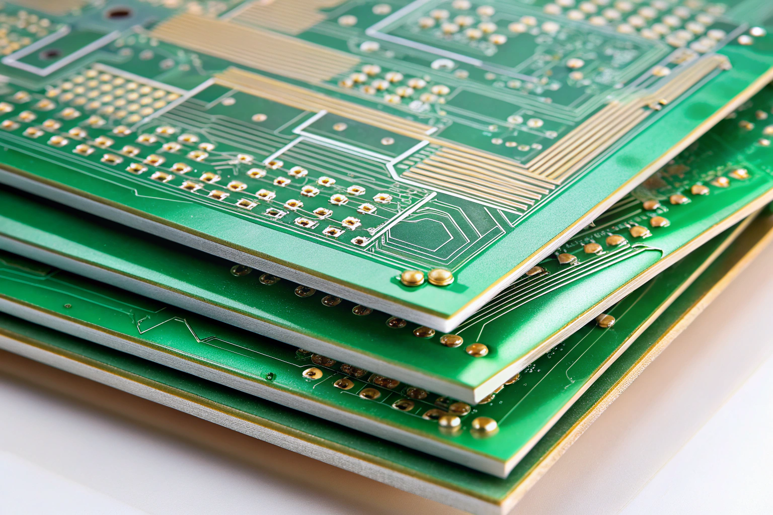
How does lamination and drilling shape the board structure?
Lamination bonds inner layers together to form the multilayer board stack.
Inner layers, prepregs, and copper foils are stacked according to the defined structure and pressed under high temperature and pressure. This creates a solid, unified board.
After lamination, CNC drilling machines create vias and through holes. Hole accuracy affects plating quality and component fit. Drill wear, speed, and alignment are closely monitored.
Factories with stable lamination and drilling processes achieve better layer registration and stronger via reliability, which is essential for high-density and multilayer designs.
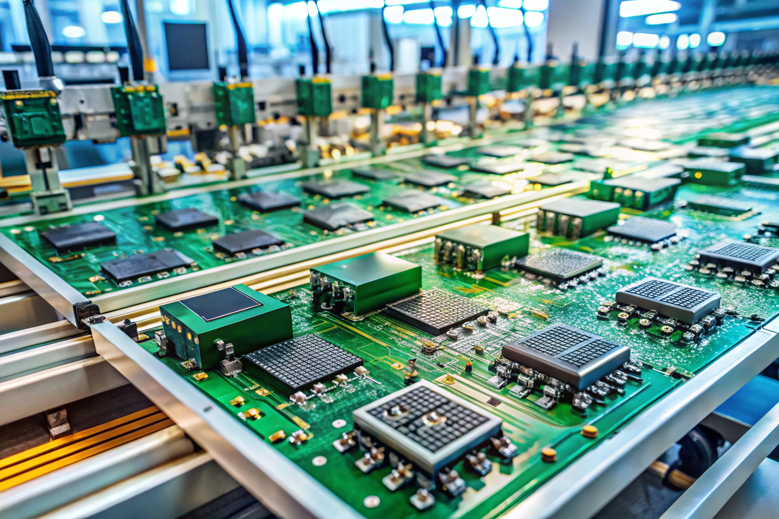
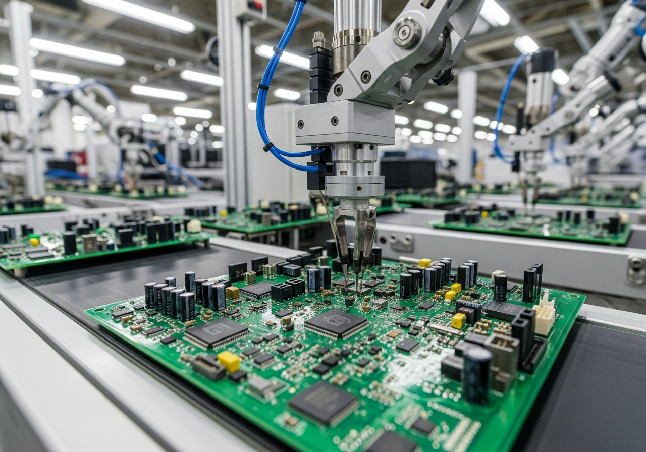
How are copper plating and outer layer circuits formed?
Drilled boards move to the plating process.
Through holes are metallized using electroless copper plating, followed by electroplating to build copper thickness. This creates electrical connections between layers.
Outer layer circuits are then imaged and etched using similar methods as inner layers. Copper thickness uniformity and adhesion are key quality indicators.
Proper plating ensures low resistance connections and strong mechanical strength. Poor plating control can lead to open circuits or reliability issues during thermal cycling.
How are solder mask, surface finish, and silkscreen applied?
After circuit formation, protective and functional layers are added.
Solder mask is applied to insulate copper traces and prevent solder bridging during assembly. Mask alignment and thickness are carefully controlled.
Surface finishes such as ENIG, HASL, or OSP are applied to exposed pads to improve solderability and protect copper. The choice of finish affects shelf life and assembly behavior.
Silkscreen printing adds component markings, reference designators, and logos. Clear and accurate silkscreen improves assembly efficiency and inspection accuracy.
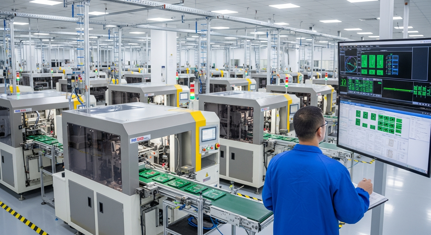
How does testing and quality control finalize PCB manufacturing?
Before shipment, finished PCBs undergo electrical testing and final inspection.
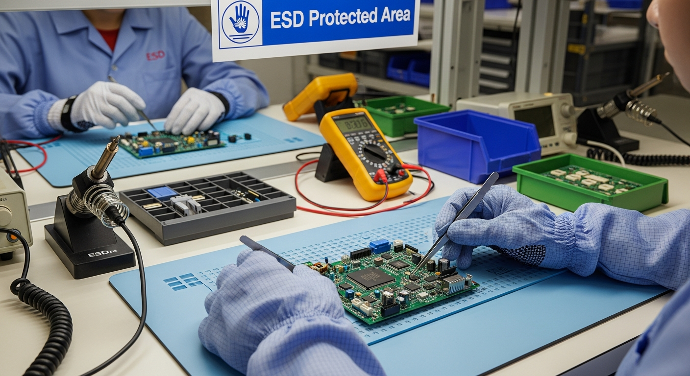
Electrical tests verify continuity and isolation, ensuring that all nets are correctly connected. Visual inspection checks board outline, surface quality, and labeling.
Quality records are reviewed to confirm process compliance. Boards that meet all requirements are cleaned, packed, and prepared for delivery using moisture-proof and anti-static packaging.
A complete quality system ensures traceability from raw materials to finished boards, supporting consistent performance and reliable downstream assembly.
Conclusion
PCB manufacturing is a comprehensive industrial process that integrates engineering, materials, precision equipment, and disciplined workshop control. From design data review and material preparation to lamination, plating, and final testing, every step builds toward electrical reliability and structural stability.
A well-defined PCB manufacturing process reduces defects, improves yield, and ensures compatibility with assembly operations. When each stage is executed under controlled conditions, the final PCB becomes a dependable foundation for electronic products throughout their entire service life.
