
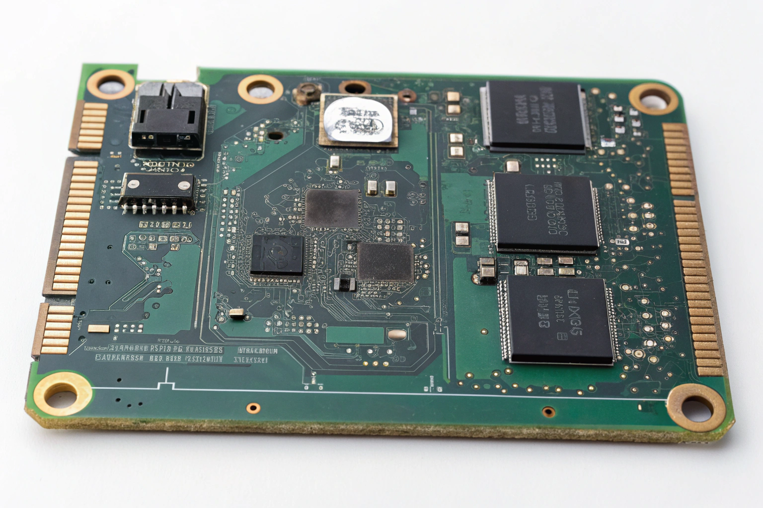
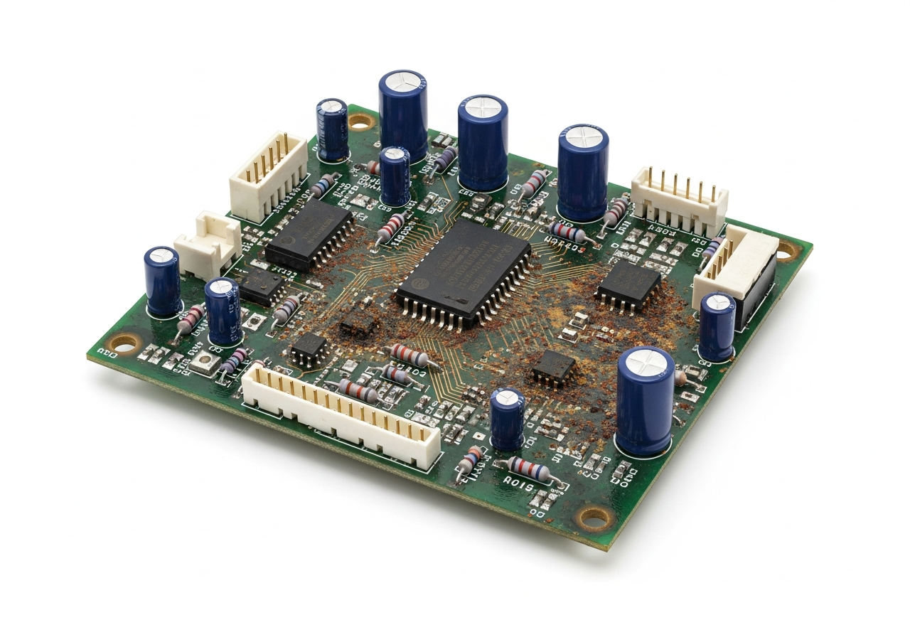
A PCB is damaged when its electrical, mechanical, or material integrity is compromised. Common signs include visible defects, abnormal electrical behavior, overheating, or intermittent operation. Some damage is obvious, while other damage is hidden and only appears under stress or testing.
PCB damage is not always catastrophic at first. Many boards continue working temporarily before failing completely. Identifying damage early is critical for troubleshooting, repair decisions, and long-term reliability.
In manufacturing and assembly environments, PCB damage detection follows structured inspection and testing steps rather than guesswork.
What Visual Signs Indicate a Damaged PCB?
Visual inspection is always the first step.
Many failures leave physical traces.
Common visible signs of PCB damage include:
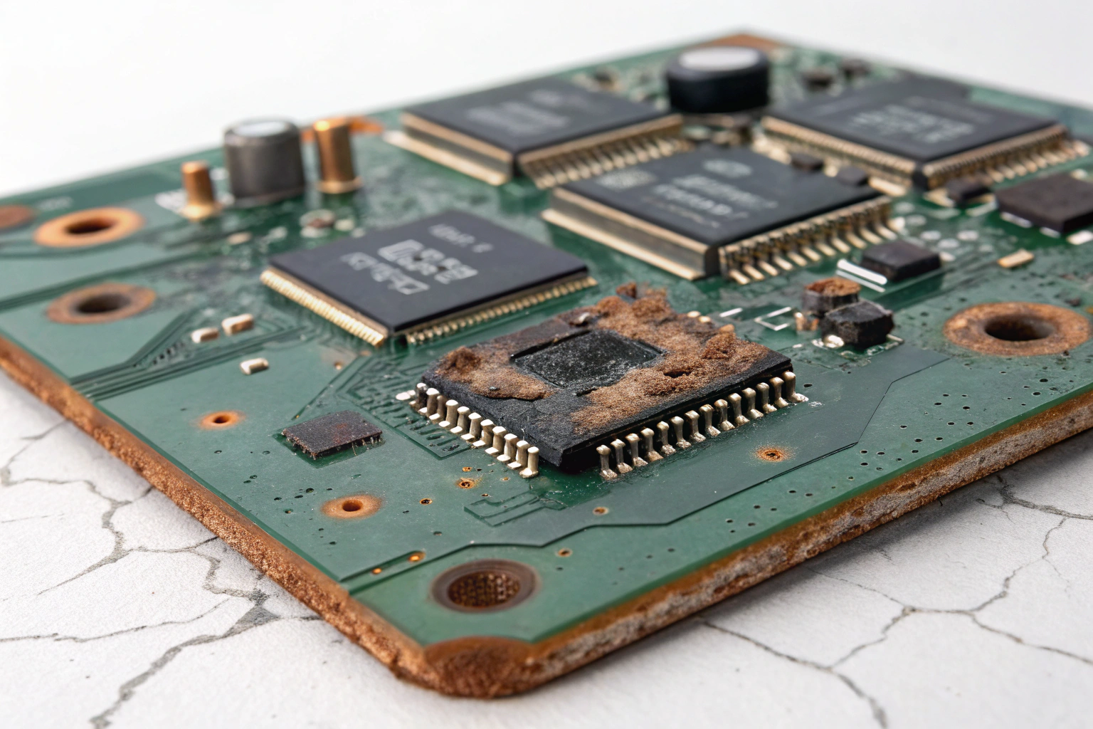
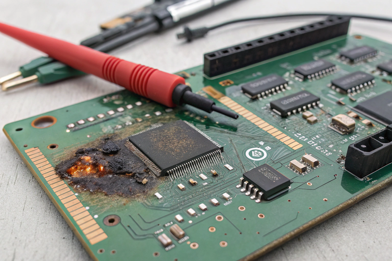
- Burn marks or discoloration
- Cracked or lifted pads
- Broken or scratched copper traces
- Bulging or leaking components
- Solder bridges or missing solder joints
Darkened areas often indicate overheating or short circuits. White residue may suggest flux contamination or corrosion. Green or black spots can point to moisture damage or chemical reaction.
In factory workshops, boards are inspected under magnification. Microscopes reveal micro-cracks, hairline trace breaks, and solder joint defects that are invisible to the naked eye.
If the PCB laminate shows charring or carbonization, the damage is considered severe. Carbonized material becomes conductive and cannot be reliably repaired. In such cases, the board is usually scrapped.
How Electrical Symptoms Reveal Hidden PCB Damage?
Not all damage can be seen.
Electrical behavior often tells the real story.
Electrical symptoms of a damaged PCB include:
- Device not powering on
- Intermittent operation
- Unstable signals or noise
- Unexpected resets or shutdowns
- Abnormal current draw
Intermittent faults are especially common. A cracked solder joint or fractured via may only fail when the board heats up or cools down.
In professional environments, multimeters, oscilloscopes, and continuity testers are used to isolate faults. Voltage drop testing helps locate high-resistance joints. Thermal cameras may reveal hot spots caused by shorts or failing components.
Electrical symptoms without visible damage often point to internal layer issues or micro-cracks that require deeper analysis.
How Solder Joint Condition Indicates PCB Health?
Solder joints are the most failure-prone points.
Their condition reflects overall quality.
Damaged or failing solder joints often show:
- Dull or grainy surfaces
- Cracks around component leads
- Insufficient or uneven solder
- Lifted joints under stress
Even joints that look acceptable can fail internally. Repeated thermal cycling causes micro-cracks that grow over time.
In manufacturing, solder joint inspection uses AOI and sometimes X-ray systems. These tools detect voids, head-in-pillow defects, and insufficient wetting under components such as BGAs.
If pressing lightly on a component causes the circuit to reconnect or disconnect, solder joint damage is highly likely.
How PCB Warping and Delamination Signal Damage?
Mechanical deformation is a serious warning sign.
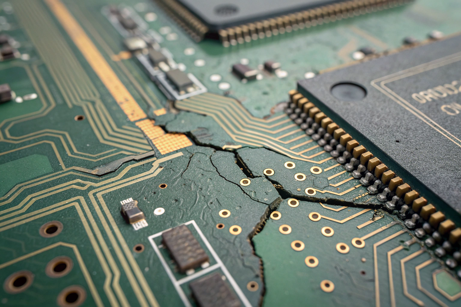
It affects both assembly and performance.
A damaged PCB may show:
- Board warping or bending
- Separation between layers
- Blisters or bubbles on the surface
Warping stresses solder joints and components, leading to secondary failures. Delamination reduces structural strength and disrupts internal copper layers.
These issues often result from excessive heat, improper reflow profiles, or poor laminate quality. Once delamination occurs, repair is rarely reliable.
In factory inspections, flatness is checked using reference surfaces or gauges. Any board exceeding flatness tolerance is rejected to prevent future failures.
How Moisture and Corrosion Damage a PCB?
Moisture is a silent but destructive factor.
Its effects appear slowly.
Moisture damage can cause:
- Corrosion on copper traces
- Green or white residue on pads
- Reduced insulation resistance
- Electrical leakage and shorts
Corrosion often starts under components or connectors where it is hard to see. Over time, copper is eaten away, breaking traces or vias.
In manufacturing, moisture-sensitive components are baked and stored in dry cabinets. Finished boards may receive conformal coating to protect against humidity.
Once corrosion reaches internal layers, the PCB is usually beyond repair.
How Factory Testing Confirms PCB Damage?
Testing turns suspicion into evidence.

Data replaces assumptions.
Professional PCB damage detection relies on testing methods such as:
- Continuity and isolation testing
- In-circuit testing (ICT)
- Functional testing under load
- Thermal stress testing
These tests reveal faults that visual inspection cannot catch. A board that passes basic power checks may still fail under full operating conditions.
In manufacturing workshops, failed test results are logged and analyzed. Repeated failures trigger root cause analysis to prevent recurrence.
Testing does not just find damage. It defines whether repair is technically and economically justified.
When Is a PCB Considered Beyond Repair?
Some damage cannot be reversed.
Replacement becomes the safer option.
A PCB is generally considered beyond repair when:
- The laminate is burned or carbonized
- Internal layers are damaged
- Multiple critical pads are lifted
- Electrical insulation is compromised
- Reliability cannot be guaranteed
In these cases, even if temporary fixes restore function, long-term failure risk remains high.
Manufacturing decisions prioritize stability and traceability over short-term recovery. Scrapping a damaged PCB often prevents larger system failures later.
Conclusion
A damaged PCB can be identified through visual inspection, electrical symptoms, solder joint evaluation, mechanical condition, and moisture or corrosion signs. While some damage is obvious, many failures are hidden and only appear through testing or under stress. In professional manufacturing, PCB damage detection follows structured inspection and validation processes to protect reliability. Early identification helps determine whether repair is acceptable or replacement is necessary. Understanding these signs reduces troubleshooting time, prevents repeated failures, and ensures electronic products perform reliably throughout their intended lifespan.
