
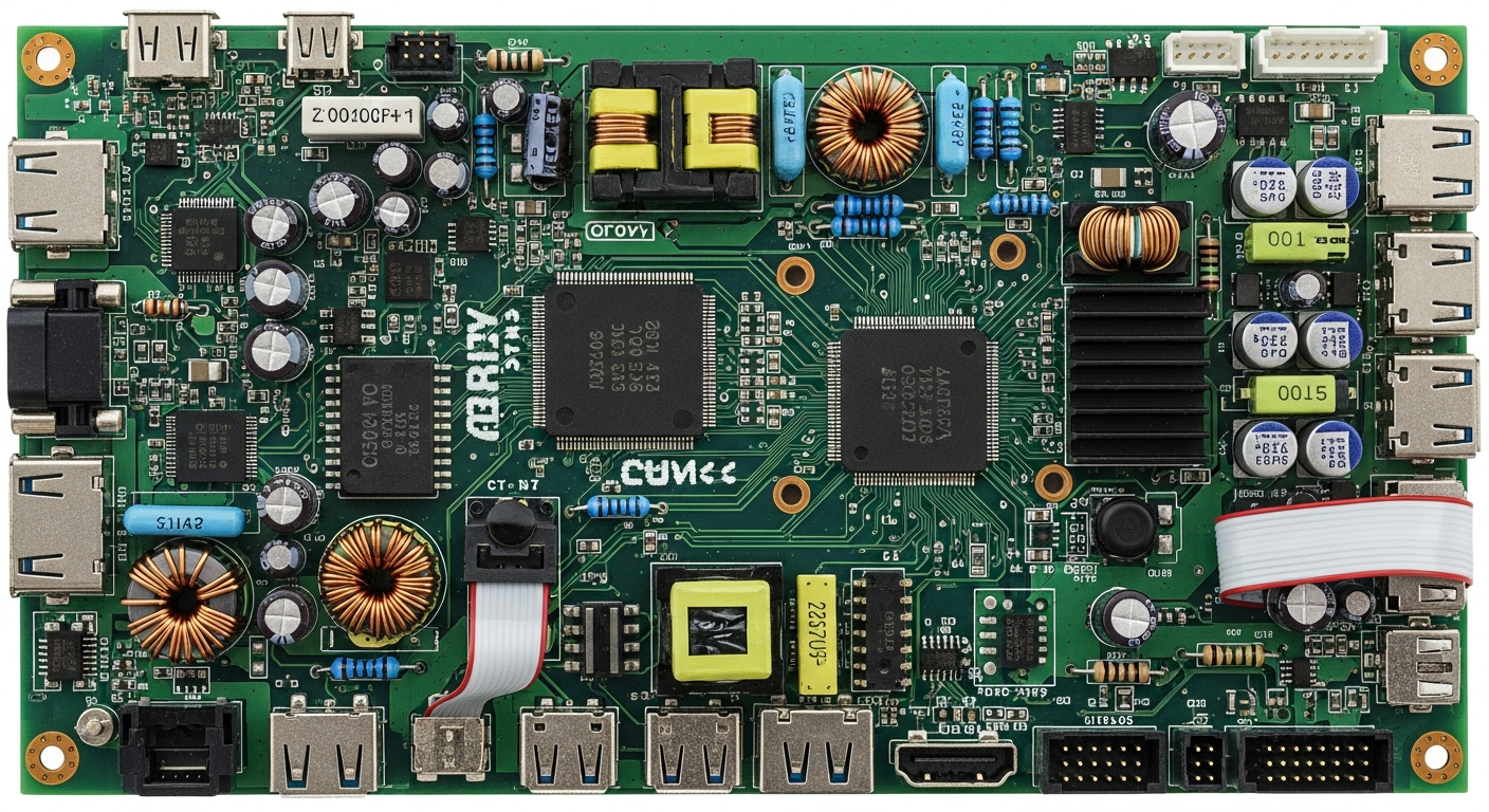
A circuit board contains several coordinated elements that work together to enable stable electrical performance. The main parts include the base material, conductive layers, components, and protective structures.
A clear understanding of each part helps engineers make better design decisions and ensures reliable manufacturing. This overview leads directly into the functional details of every major section found on modern PCB and PCBA assemblies.
What are the primary structural parts of a circuit board?
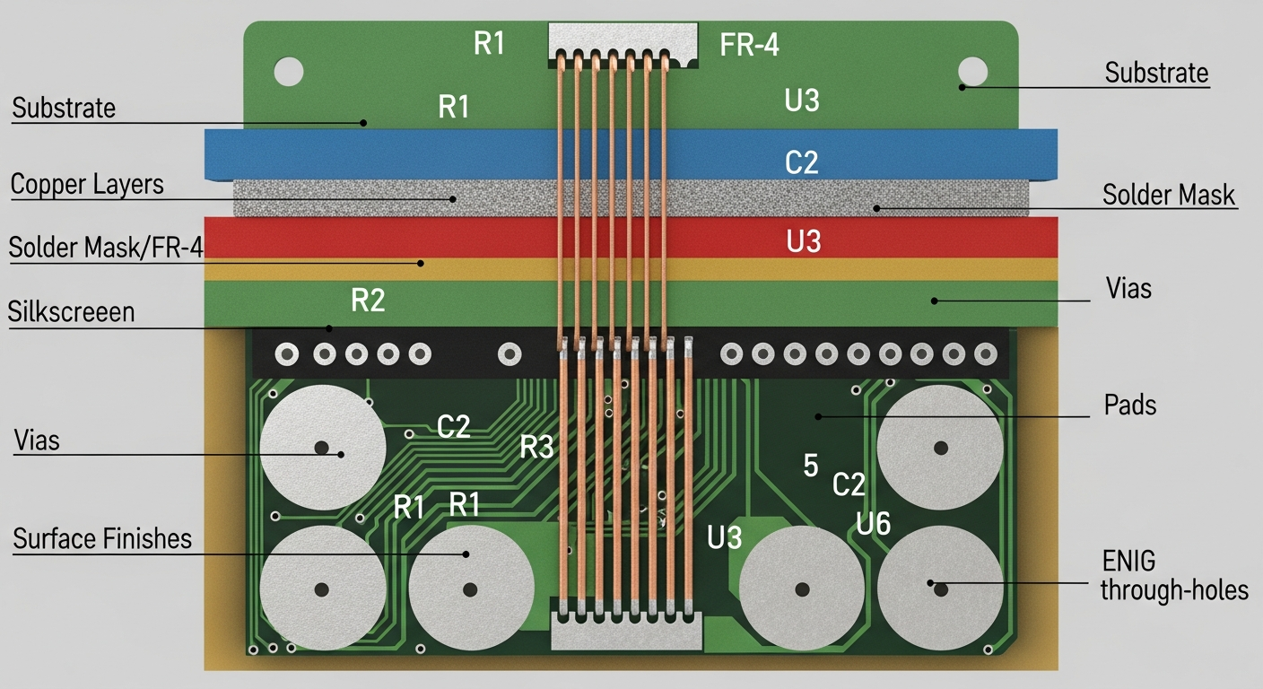
A circuit board’s structure relies on several layers that support components, conduct signals, and withstand environmental demands.
The main structural parts are the substrate, copper layers, solder mask, silkscreen, vias, pads, and surface finishes.
Deeper Explanation and Industry Insights
Substrate (Base Material)
The substrate forms the board’s backbone. FR4 is the most common choice due to its strength and insulation performance. High-frequency applications may use materials such as Rogers to reduce signal loss.
Industry relevance: Product stability depends heavily on the substrate. Poor-quality boards may warp, absorb moisture, or crack during soldering.
Copper Layers
Copper layers carry current and signals. Multilayer PCBs allow more routing density, improved grounding, and EMI control.
Buyer pain point: Incorrect copper thickness or poor lamination can cause overheating, broken traces, and early field failures.
Factory advantage: Controlled lamination processes and strict IPC-A-610 standards ensure consistent copper quality across prototypes and production.
Solder Mask
The solder mask protects copper from oxidation and prevents solder bridges. Green is common, but other colors are widely used for branding or inspection requirements.
Buyer concern: Uneven solder mask thickness can create defects during SMT placement.
Manufacturing benefit: Automated exposure and AOI scanning ensure clean apertures and repeatable results.
Silkscreen
Silkscreen markings guide assembly and repair processes. They identify components, test points, and polarity marks.
Factory value: Accurate silkscreen printing reduces assembly errors and speeds up debugging during product validation.
Vias and Pads
Vias connect different copper layers, while pads provide component mounting points.
Buyer challenge: Incorrect via tenting or pad design may cause solder wicking or open circuits.
Engineering support: DFM review highlights issues early, ensuring trouble-free SMT and DIP assembly later.
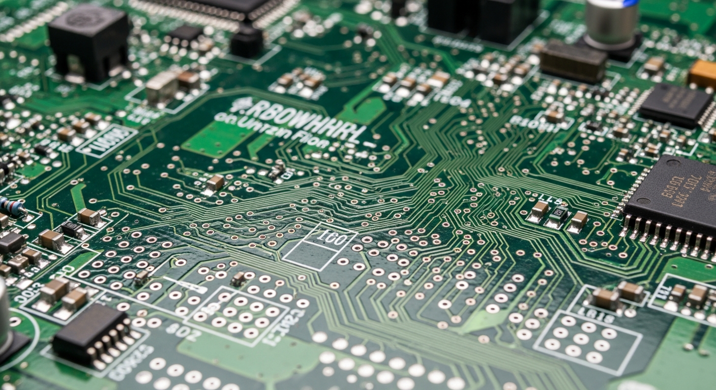
How do electrical components function on a circuit board?
Electrical components shape signals, manage power, and define a product’s complete behavior.
Electrical components include passive parts, active semiconductors, connectors, sensors, and power modules.
Deeper Explanation and Industry Insights
Passive Components
Resistors, capacitors, and inductors guide basic electrical functions. They stabilize signals, store energy, or filter noise.
B2B concern: Wrong substitution or poor-quality passives cause drift, noise, or unstable performance.
Manufacturing advantage: Verified component sourcing and approved vendor lists help maintain consistency across batches.
Active Components
Microcontrollers, ICs, transistors, and drivers define logic and processing power. Component packaging—QFN, BGA, LGA—often requires fine-pitch assembly accuracy.
Pain point: Incorrect reflow profiles or insufficient inspection can lead to BGA voids or hidden solder issues.
Factory solution: Precise ±0.03 mm SMT placement accuracy and X-ray inspection ensure secure solder joints.
Connectors
Connectors bridge the board with external modules, power supplies, or mechanical interfaces.
Customer issue: Connector misalignment or weak soldering causes field failures due to vibration or handling.
Factory capability: Reinforced soldering techniques and testing procedures maintain mechanical strength.
Sensors and Modules
Wireless modules, temperature sensors, and MEMS elements enhance system intelligence.
Industry need: Sensitive devices require ESD protection, shielding, and careful handling.
Factory practice: Dedicated ESD zones and moisture-sensitive component baking safeguard performance.
What role does copper routing play in PCB performance?
Copper routing carries power and signals to every part of the board, shaping speed, stability, and heat distribution.
Copper routing defines signal paths, grounding networks, and power delivery to ensure low loss and high reliability.
Deeper Explanation and Industry Insights
Signal Traces
Signal traces determine how data travels. High-speed traces must follow controlled impedance rules, matched lengths, and shielding patterns.
Buyer frustration: Poor routing can cause crosstalk, reflection, or timing errors.
Engineering support: Detailed DFM reviews and impedance calculations help prevent routing-related failures.
Power Traces
Power sections require thicker copper, wide pours, and optimized thermal paths.
Pain point: Overheated power lines may lead to burnt boards or unstable voltage.
Factory advantage: Adjustable copper thickness (1–3 oz) and thermal simulation ensure safe current capacity.
Grounding and EMI
Ground planes reduce noise, support EMC compliance, and stabilize RF behavior.
Buyer challenge: Many designs fail certification due to poor grounding.
OEM experience: Strong grounding strategies guided by real production cases shorten certification timelines.
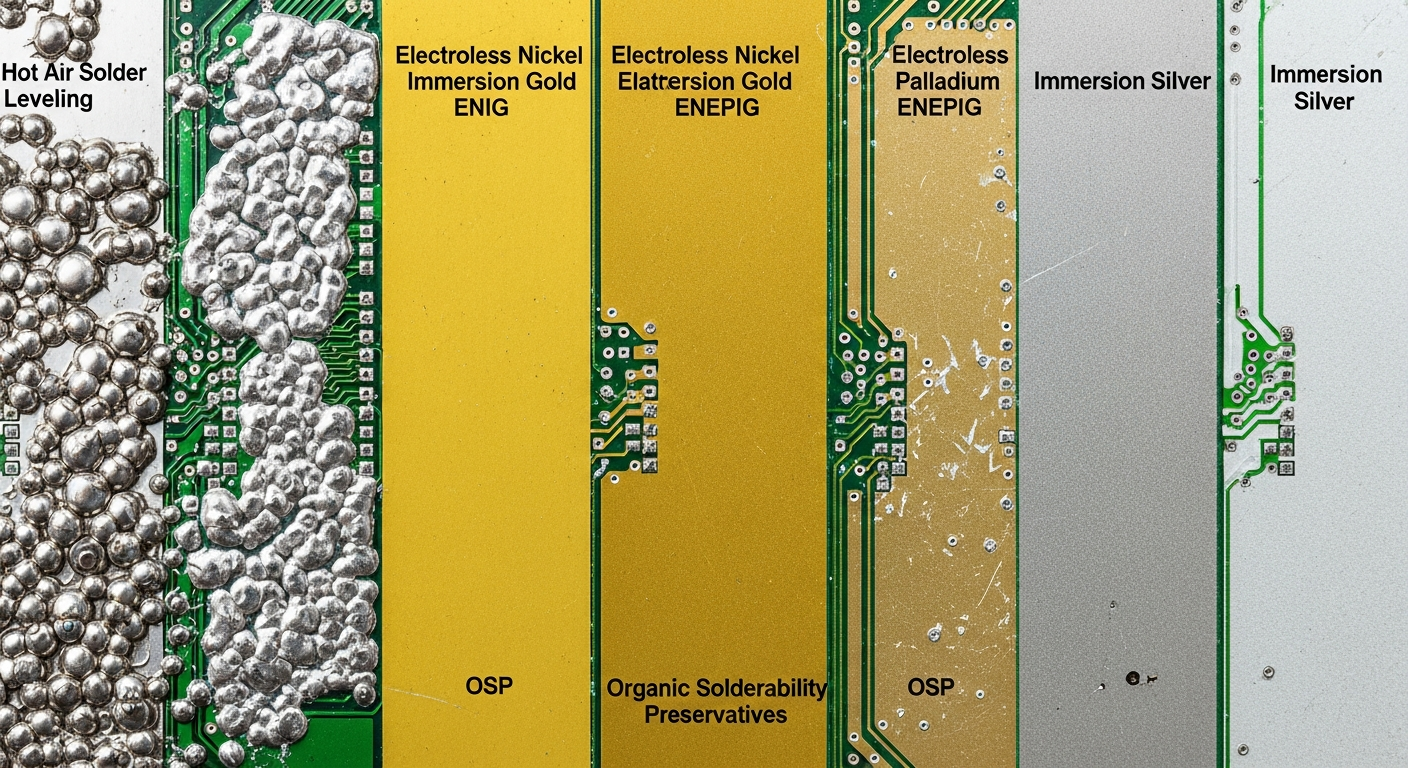
Why are surface finishes important in PCB manufacturing?
Surface finishes protect exposed copper and ensure strong solder joints during assembly.
Common finishes include HASL, ENIG, ENEPIG, OSP, and immersion silver, each suited for different applications.
Deeper Explanation and Industry Insights
Finish Types
- HASL (Lead-free Hot Air Solder Leveling): Cost-effective, general use
- ENIG (Electroless Nickel Immersion Gold): Flat pads for fine-pitch SMT
- ENEPIG: Good for wire-bonding and mixed-technology builds
- OSP: Simple, organic protection for copper
- Immersion Silver: Good for high-frequency performance
Buyer Pain Points
Unsuitable finishes lead to solderability defects, oxidation, voiding, or degraded RF behavior. Many low-tier suppliers cut corners in plating thickness or quality control.
Factory Advantage
Strict plating bath management, full-process traceability, and finish selection guidance based on product use cases reduce risk and improve long-term durability.
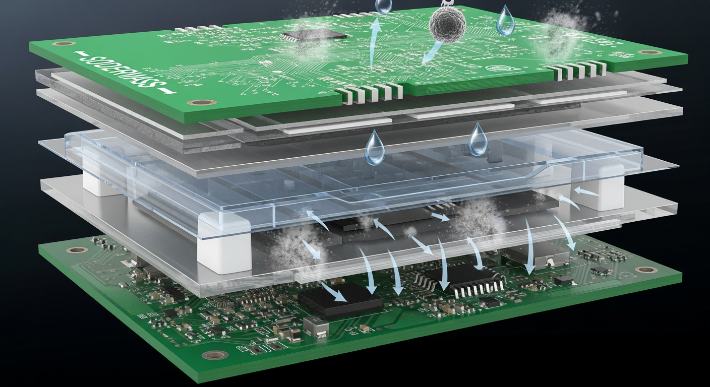
How do protective layers improve board reliability?
Protection extends a circuit board’s lifespan by shielding it from moisture, dust, scratches, and mechanical stress.
Protective layers include solder mask, conformal coating, and specialized encapsulation materials.
Deeper Explanation and Industry Insights
Conformal Coating
Acrylic, silicone, or urethane coatings protect sensitive electronics in harsh environments.
B2B issue: Uneven coating or contamination leads to corrosion or short circuits.
Factory edge: Automated coating systems create a uniform protective layer.
Encapsulation
Potting compounds add more robust protection for automotive, industrial, or outdoor devices.
Buyer challenge: Excessive heat trapping or poor material compatibility.
Engineering guidance: Material selection rules and thermal analysis minimize risk.
Mechanical Reinforcement
Edge stiffeners, shield cans, or adhesive mounts reinforce structural stability.
Customer need: Better durability under vibration or impact.
Production expertise: Proven reinforcement steps based on real market applications.
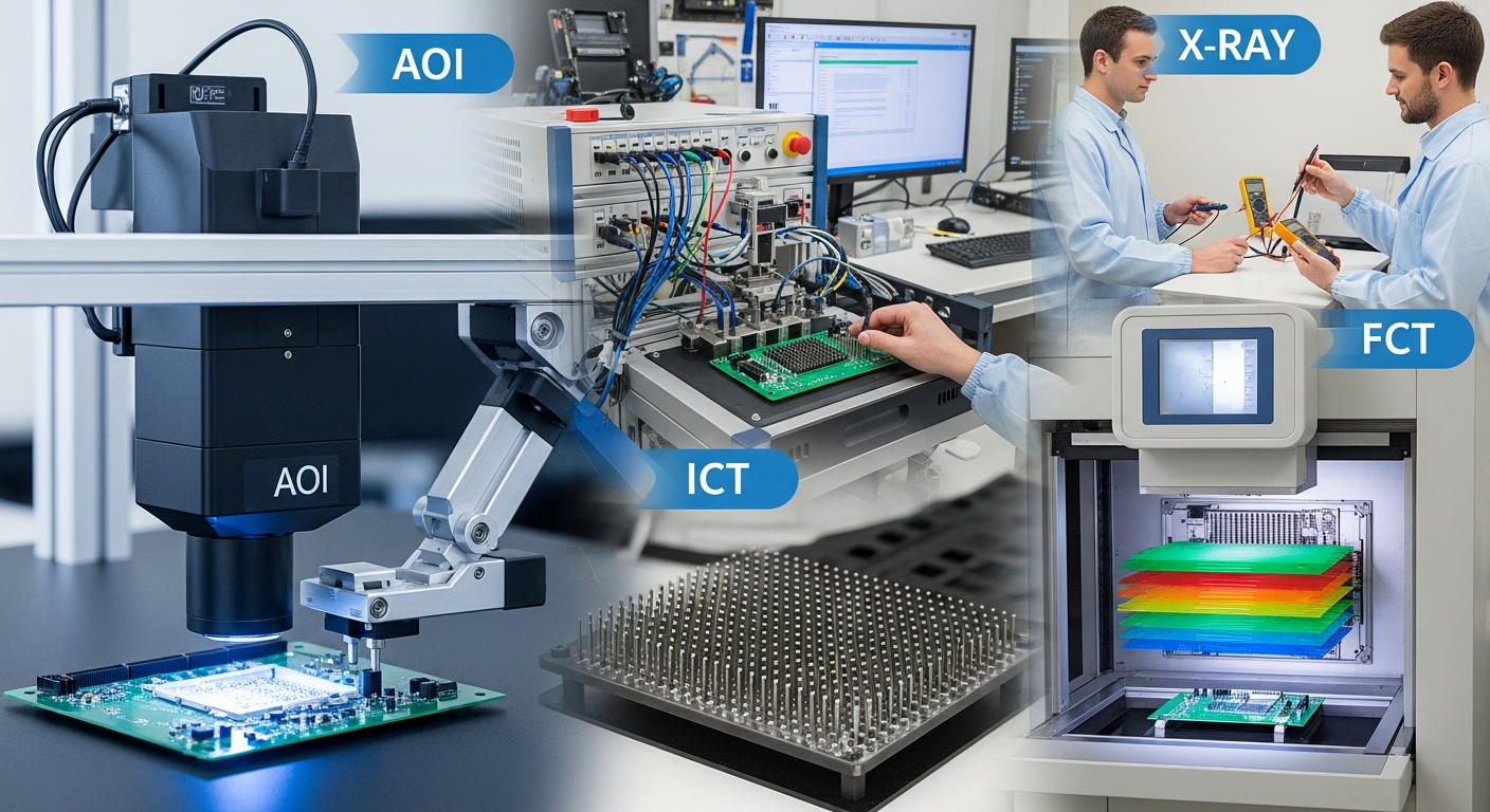
Why are testing and inspection essential parts of a circuit board?
Testing ensures every assembled board performs as intended before delivery to the customer.
Common processes include AOI, X-ray, ICT, FCT, and final functional validation.
Deeper Explanation and Industry Insights
AOI (Automated Optical Inspection)
AOI detects misaligned components, missing parts, and solder defects.
Pain point: Manual checks miss tiny issues.
Factory advantage: High-resolution AOI for 0201 and fine-pitch devices.
X-ray
Used for BGAs and internal solder visibility.
Buyer concern: Hidden defects cause intermittent failures.
Factory reassurance: Full-area scanning ensures secure assembly.
ICT & FCT
ICT examines electrical connectivity, while FCT validates functionality.
Customer expectation: Every board must work exactly as designed.
Factory strength: Customized test fixtures and complete reporting (AOI, FCT, packaging photos) keep every step transparent.
Conclusion
Circuit boards combine structural layers, conductive paths, protective coatings, and electronic components to create a reliable foundation for modern devices. Each part plays a defined role in stability, signal quality, heat control, and long-term durability. Careful material selection, precise routing, strict inspection, and professional manufacturing practices ensure consistent results from prototype to mass production. Detailed engineering support, clear documentation, and repeatable processes help reduce development risks and keep production stable across every stage of a product’s lifecycle. This complete approach allows new hardware designs to move faster, perform better, and maintain strong reliability in real-world conditions.
