
Using one fab house for both prototype and bulk production ensures consistent quality, reduced delays, and smoother scaling from early samples to volume manufacturing.
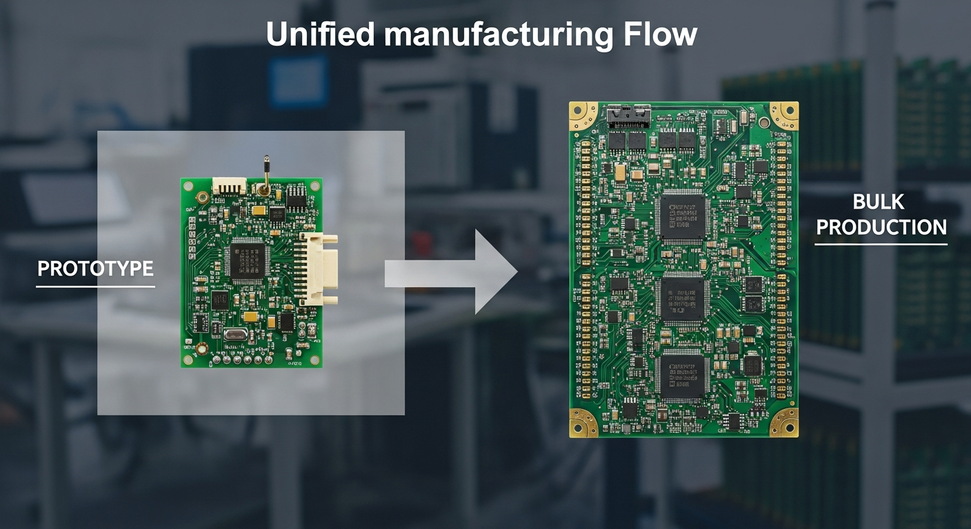
A unified manufacturing flow helps hardware teams avoid mismatched specifications, communication gaps, and repeated onboarding across multiple suppliers.
Why produce PCB prototypes and bulk orders in the same fab house?
Switching factories often causes inconsistent quality, rework, and increased engineering cost.
Producing prototypes and bulk orders in one fab house ensures continuity, stable quality, and predictable performance.

Consistent Stackup, Reliable Specs, and Smooth Scaling
A single fab house maintains the same copper thickness, solder mask type, surface finish, trace tolerance, and drilling accuracy between samples and mass production. Material consistency avoids redesigns due to different dielectric properties or warpage behavior. Process familiarity shortens DFM cycles and strengthens reliability as the product moves forward.
In B2B workflows, using multiple factories often leads to layer misalignment, altered plating thickness, or incompatible solder mask. Engineering-led facilities with both PCB fabrication and SMT assembly preserve consistent parameters across all production volumes, minimizing risk and guaranteeing predictable electrical behavior.
How does a single-source workflow reduce engineering workload?
Multiple fab transitions force teams to repeat DFM reviews, adjust stackups, and correct mismatched specifications.
A single fab house reduces rework by maintaining stable manufacturing rules throughout development.
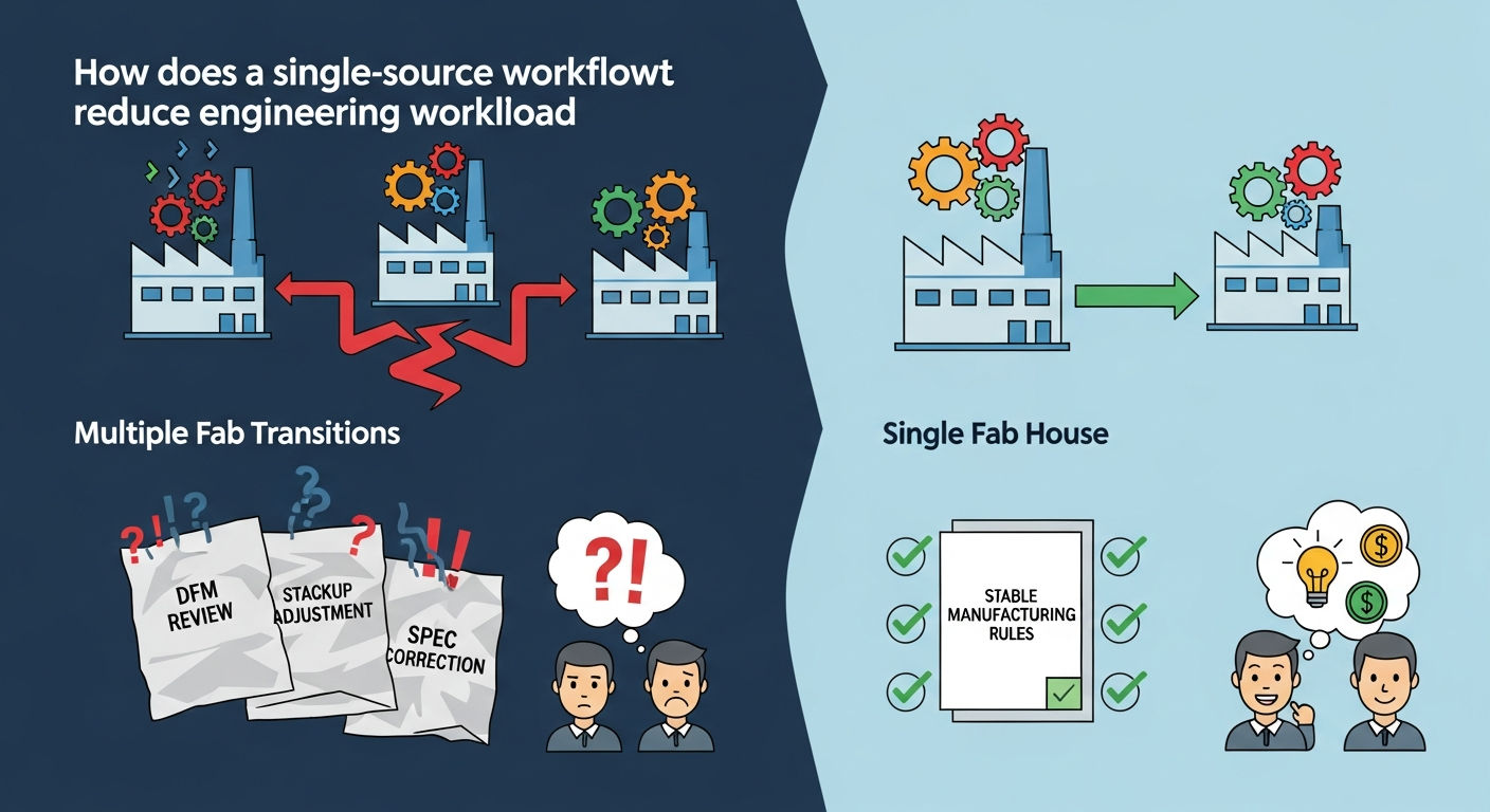
Once Gerber files, drilling data, and layer definitions are validated in the first prototype, the same parameters apply to all later runs. The engineering team no longer needs to re-check annular rings, solder mask clearances, controlled impedance rules, or mechanical outlines for a new supplier. Every revision follows the same predictable process.
Factories with OEM/ODM experience maintain internal documentation, stackup libraries, drill charts, and plating profiles. This ensures stability, reduces confusion, and accelerates the journey from initial concept to mass production. Such consistency benefits industrial, IoT, and consumer electronic projects that require tight timelines.
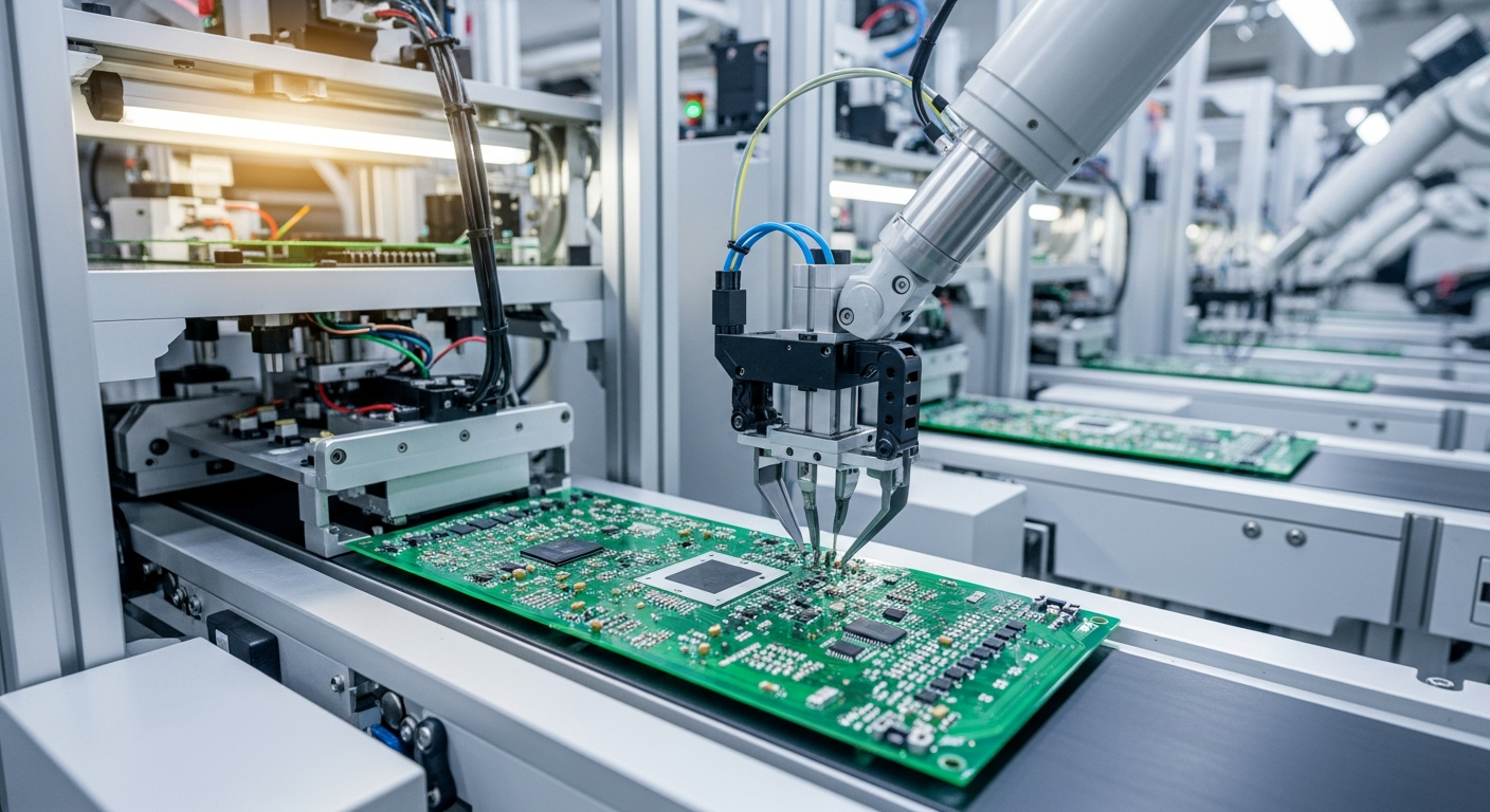
How does combining PCB fabrication and assembly strengthen quality?
Different vendors often work with different tolerances, causing solderability issues or unreliable mechanical stability.
A single fab–assembly ecosystem keeps PCB fabrication aligned with SMT/DIP process requirements.
Fabrication Rules, Pad Geometry, and Assembly Compatibility
When fabrication and assembly happen in the same facility, solder mask openings, stencil thickness, pad size, and hole tolerances are matched to actual SMT and DIP capabilities. AOI, X-ray, and FCT testing confirm the match between PCB design and assembly rules.
Factories with integrated lines catch issues such as uneven HASL surfaces, incorrect ENIG thickness, or warpage before boards reach pick-and-place machines. This alignment reduces defects and supports stable performance across all volumes.
How does a single fab house help with BOM consistency and supply-chain stability?
Working with different factories often results in varied component substitutions, inconsistent part sourcing, and unaligned quality grades.
One fab house maintains uniform BOM sourcing strategies and long-term purchasing stability.
Controlled Sourcing, Verified Alternatives, and Predictable Lead Time
A unified procurement system reviews part numbers, checks package compatibility, and monitors long-term availability. When substitutions are needed, they follow strict electrical and mechanical matching rules. Component orientation and polarity are validated once, avoiding repeated debugging.
Manufacturing partners with a global supply-chain network support cost optimization and provide early warnings for end-of-life (EOL) or allocation issues. This stability simplifies planning and protects B2B production pipelines from unexpected delays.
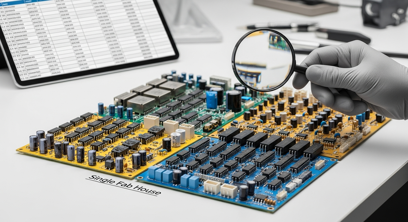
How does traceability improve when using one fab for all stages?
Multiple suppliers complicate data tracking, inspection logs, and revision control.
A single fab house provides unified traceability from PCB fabrication to final testing.
Serial Tracking, Inspection Records, and Manufacturing History
All process data—AOI results, drill maps, solder mask inspections, stencil IDs, reflow profiles, and FCT logs—remains in one integrated system. This allows fast root-cause analysis and straightforward quality audits.
Factories combining fabrication and assembly deliver packaged shipments with full documentation: COC, test results, photos, and trace codes. This consistency reduces long-term risk and supports reliable field performance.
How does one fab house accelerate time-to-market?
Fragmented vendors create delays due to mismatched capabilities, slow communication, and inconsistent revision handling.
A single fab house speeds development with fast feedback loops and synchronized workflows.
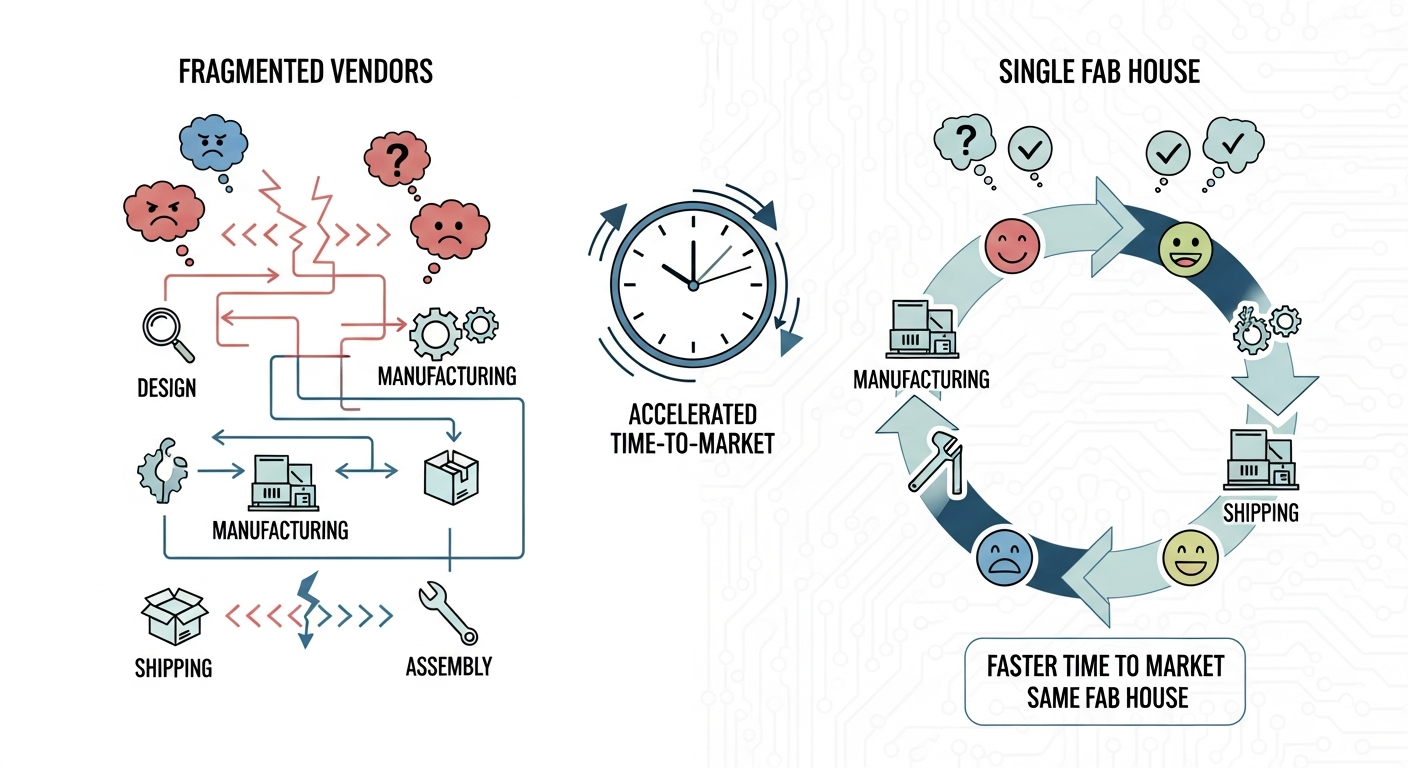
Rapid Prototyping, Fast DFM Feedback, and Revision Control
Prototypes are produced quickly, tested internally, and adjusted before rolling into small-batch production. Revision changes are applied once and follow the same guidelines in every stage. Communication stays continuous, avoiding the delays that happen when multiple vendors must be re-aligned.
Engineering-oriented facilities combine PCB production, SMT, DIP, testing, and packaging under one roof, allowing project updates to propagate instantly across departments. This is especially valuable for startups, industrial builders, and IoT teams with tight deadlines.
Conclusion
Choosing one fab house for both PCB prototypes and bulk production creates a stable, efficient, and predictable manufacturing pipeline. Unified DFM, consistent materials, synchronized PCB–SMT compatibility, and consolidated testing reduce defects and accelerate development. When supported by engineering-driven processes, global supply-chain strength, and complete testing systems, this single-source approach delivers cleaner prototypes, smoother scaling, and reliable performance across mass production. Such integration strengthens product stability and supports long-term success for industrial, IoT, automotive, and consumer electronics worldwide.
