
Many people confuse PCB and PCBA, but they represent two different stages of electronic manufacturing. Understanding their difference is key to managing product design and production efficiently.
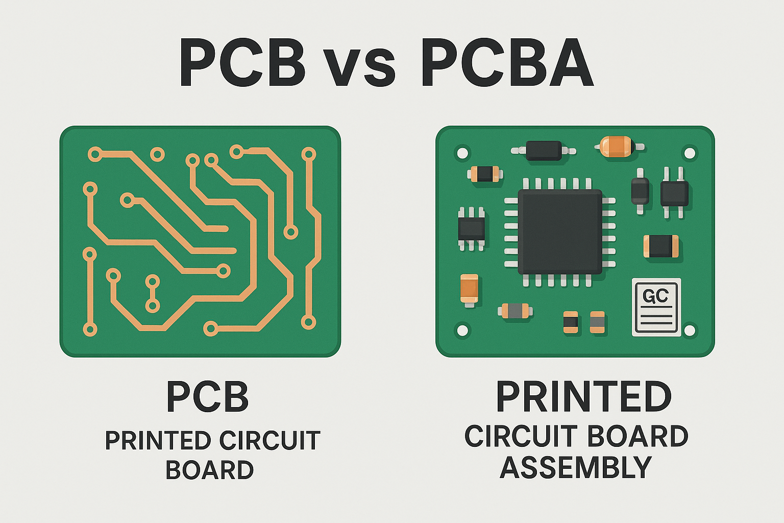
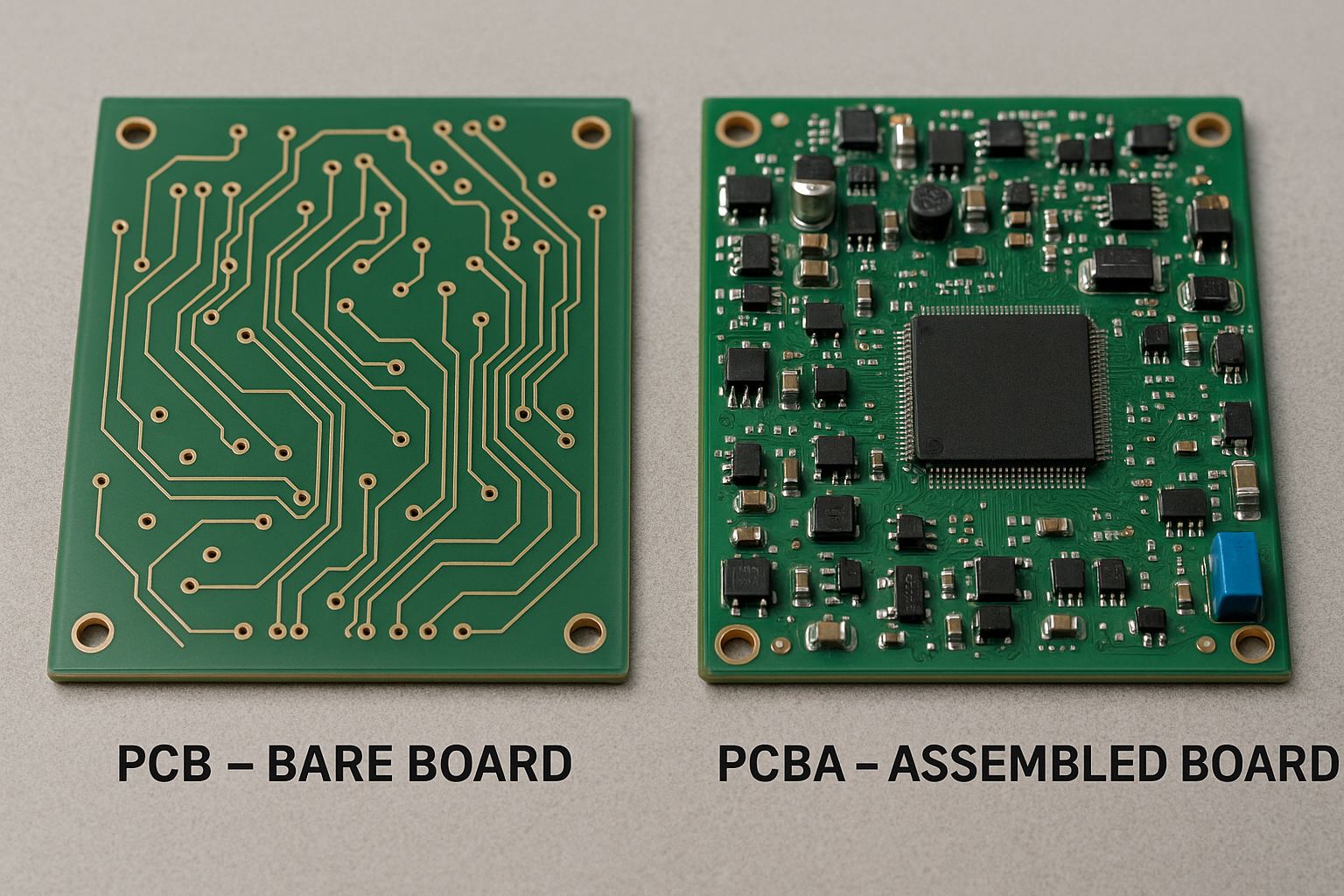
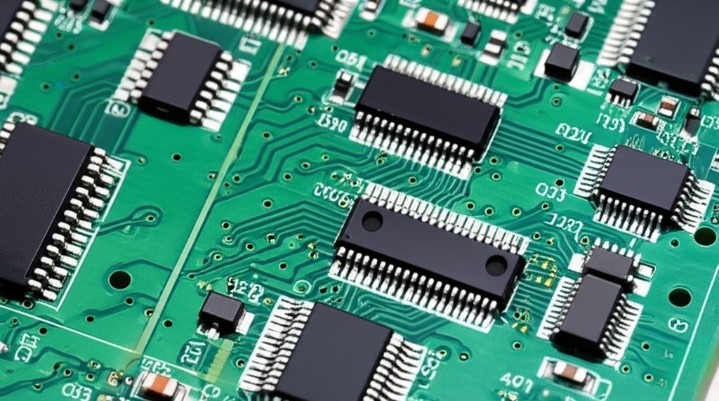
PCB refers to the bare printed circuit board without components, while PCBA (Printed Circuit Board Assembly) is the completed board with all electronic components soldered onto it.
Knowing the difference between PCB and PCBA helps engineers plan manufacturing processes, testing, and quality control. Let’s explore both terms in detail and understand how they work together in electronics production.
What is a PCB (Printed Circuit Board)?
It’s the foundation that connects all components.
A PCB is a flat board made of insulating material with copper traces that connect electronic components.
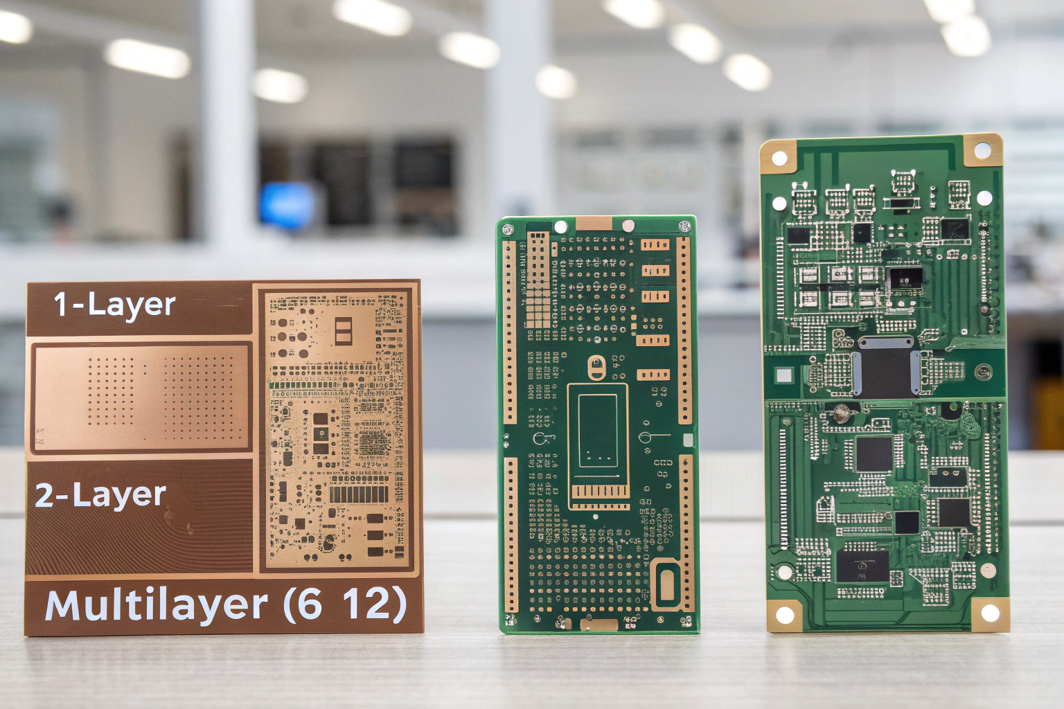
A PCB provides both mechanical support and electrical connections. It’s made by laminating copper layers onto substrates like FR4 or aluminum. The copper is etched to form conductive paths. PCBs can be single-sided, double-sided, or multilayer, depending on circuit complexity. In my factory, we produce PCBs ranging from simple 1-layer boards to complex 12-layer designs used in industrial, IoT, and communication devices.
| PCB Type | Layers | Common Use |
|---|---|---|
| Single-layer | 1 | Simple LED boards |
| Double-layer | 2 | Consumer electronics |
| Multilayer | 4–12 | Industrial and IoT systems |
A bare PCB itself cannot function—it only becomes a working circuit after assembly.
What is a PCBA (Printed Circuit Board Assembly)?
PCBA refers to the process and result of mounting and soldering all components onto the PCB to form a functional circuit board.
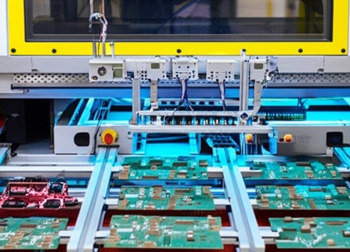
A PCBA includes resistors, capacitors, ICs, connectors, and other parts installed through SMT (Surface Mount Technology) or THT (Through-Hole Technology). After placement, the board is soldered, inspected, and tested. In our assembly lines, SMT and DIP processes are combined to complete both sides of the board. Every PCBA passes AOI, ICT, and FCT testing before shipment to ensure full functionality.
| Process Step | Description |
|---|---|
| SMT Assembly | Solder paste printing, component placement, reflow |
| DIP Insertion | Through-hole component soldering |
| Testing | AOI, ICT, and functional tests |
| Final Inspection | Visual check and packaging |
What is the main difference between PCB and PCBA?
One is the base, the other is the finished product.
A PCB is an empty board with copper traces, while a PCBA is the assembled board with components ready to operate.
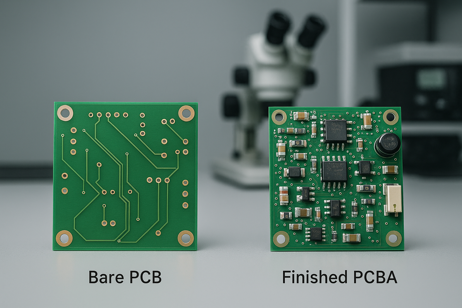
Think of PCB as a “skeleton” and PCBA as the “complete body.” The PCB manufacturing involves design, etching, drilling, and finishing, while PCBA involves mounting, soldering, and testing. PCB fabrication focuses on materials and layout precision; PCBA focuses on assembly accuracy and component reliability.
| Comparison | PCB | PCBA |
|---|---|---|
| Meaning | Bare circuit board | Assembled, functional board |
| Components | None | All mounted parts |
| Production Process | Fabrication | Assembly & Soldering |
| Functionality | Passive | Active & operational |
| Typical Users | PCB manufacturers | Assembly factories or EMS providers |
In my factory, both PCB fabrication and PCBA assembly are done under one roof, which ensures better coordination, faster delivery, and consistent quality control.
How is a PCB made before becoming a PCBA?
PCB manufacturing includes circuit imaging, etching, drilling, plating, solder mask, silkscreen, and surface finish.
Once the Gerber files are received, engineers review the design and prepare photomasks. The copper layers are etched to form traces, holes are drilled and plated, and a protective solder mask is applied. Finally, finishes like ENIG or HASL are added for better solderability. Only after these steps can the PCB be sent to the assembly line for component placement.
| Process Step | Purpose |
|---|---|
| Imaging & Etching | Create copper traces |
| Drilling & Plating | Form via connections |
| Solder Mask | Protect copper |
| Surface Finish | Improve solderability |
This stage ensures the base quality of the entire PCBA process.
What happens during PCBA assembly?
Precision machines bring the circuit to life.
The PCBA process involves solder paste printing, pick-and-place, reflow soldering, inspection, and functional testing.
Solder paste is applied to pads using a stencil. Components are then automatically placed by SMT machines. The board goes through a reflow oven, where the paste melts and solidifies, forming reliable solder joints. Through-hole components are inserted and soldered afterward. Finally, AOI and testing confirm the assembly’s performance. In our lines, this process is supported by Yamaha SMT machines capable of 0201 packages, with ±0.03 mm accuracy and 24-hour engineering feedback.
| Stage | Equipment | Quality Control |
|---|---|---|
| Solder Paste Printing | Stencil printer | Paste thickness check |
| Placement | Pick & place machine | Vision alignment |
| Reflow | 10-zone oven | Temperature profiling |
| Testing | AOI & FCT | Electrical verification |
PCB vs PCBA cost – What affects the price?
PCB cost depends on layer count, material, and finish; PCBA cost depends on components, assembly process, and testing.
For example, a 4-layer FR4 PCB may cost only a few dollars per piece, but once components, soldering, and testing are added, the PCBA can cost several times more. High-precision components, fine-pitch ICs, or complex testing increase assembly cost. In my experience, combining PCB and PCBA production in one facility reduces logistics time and helps control the total project cost.
| Cost Factor | PCB | PCBA |
|---|---|---|
| Material | FR4, Rogers, Aluminum | Depends on BOM |
| Process | Etching, drilling | SMT, Reflow, Testing |
| Labor | Low | Medium to high |
| Typical Cost | Low | Higher due to assembly |
Conclusion
PCB is the essential base, while PCBA is the complete functional assembly. Both are vital stages of electronic manufacturing. Understanding their difference helps you plan production, quality control, and cost more effectively. In my factory, we deliver both PCB fabrication and PCBA assembly to ensure seamless coordination, fast delivery, and high-quality results for every electronic project.
