
At CustomPCBA, we specialize in providing PCBA assembly solutions for critical applications. From advanced devices to complex diagnostic equipment, we ensure precision, reliability, and compliance with rigorous industry standards.

Fast and precise prototyping services for complex circuit board designs—ideal for R&D, pilot production, and function verification. We help you reduce development risks, validate performance early, and accelerate time-to-market.
Custom solutions for small-batch PCB assembly of industrial, automotive, or IoT devices. We support flexible order quantities, engineering support, BOM validation, and quick turnaround for fast-paced product development.
From component sourcing and PCB fabrication to assembly, functional testing, and packaging—we offer full-process PCBA manufacturing with cost control, complete traceability, and smooth, reliable end-to-end project execution.
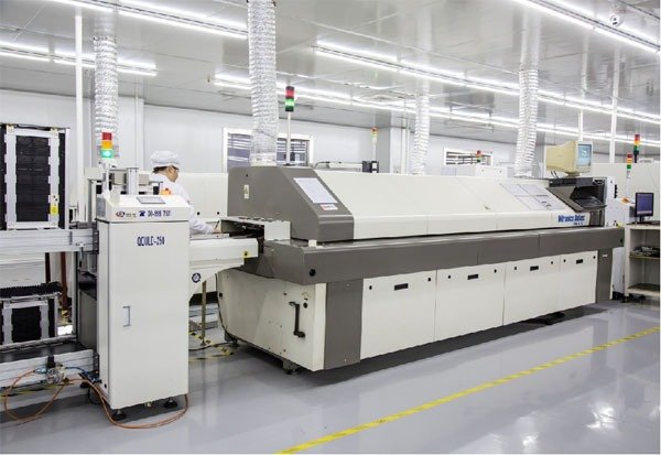
High-efficiency and scalable PCBA services for mass production. With advanced automated SMT lines, inline AOI/X-ray inspection, and MES tracking, we ensure consistent output, stable quality, and reliable delivery for large-volume needs.
01005, 0201, CSP, WLP, Flip-Chip
0.35mm pitch BGA, QFN, PoP, SiP
Exceptional BGA First Pass Yield Rate
99% Satisfaction Across Batches
01005, 0201, CSP, WLP, Flip-Chip
0.35mm pitch BGA, QFN, PoP, SiP
Exceptional BGA First Pass Yield Rate
99% Satisfaction Across Batches
SMT 01005 or largerCable & wire
BGA 0.35mm pitch, POP (Package on Package)
WLCSP 0.35mm pitch
Chip: min 01005
IC/Pedestal: min pitch 0.3
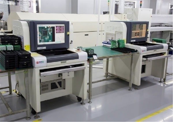
3D AOI
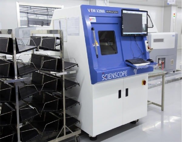
X-ray
FAI
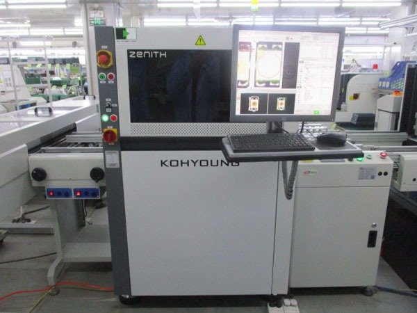
SPI
50X Microscope
| Capability / Feature | Typical Range / Notes |
|---|---|
| Layer count | Standard: 1–16 layers; Advanced: up to 32 layers (some fabs support 40+ or “any layer” structures). |
| Board thickness | 0.4–4.5 mm overall. Common FR‑4 options: 0.4/0.6/0.8/1.0/1.2/1.6/2.0 mm; 2.5 mm+ for 12‑layer boards and above. R&D builds can go down to 0.20 mm. |
| Max/min board size | Standard: up to ≈600 × 570 mm; Advanced: 960 × 600 mm; R&D: 1250 × 570 mm. Min board: 50 × 50 mm (standard), 30 × 30 mm (advanced), 5 × 5 mm (R&D). |
| Min trace/space | Standard: ≈3 mil/3 mil (0.075 mm); Advanced: 2.5 mil/2.5 mil (0.063 mm); HDI/RF: 2 mil/2 mil (0.05 mm). On 1‑oz copper, down to 0.09 mm on 4‑layer boards. |
| Min via / drill diameters | Through‑holes: 0.15–0.30 mm multilayer; 0.65 mm aluminium‑core; 1 mm copper‑core. Laser/microvia: 0.075 mm standard, 0.065 mm advanced. Min NPTH: 0.50 mm. |
| Aspect ratio (board thickness : hole diameter) | Standard 10:1, Advanced 16:1, R&D 20:1. |
| Copper weights | Outer layers: standard up to 3 oz; advanced up to 12 oz; R&D > 12 oz. Inner layers similar. High‑power options: outer 1–2 oz, inner 0.5/1/2 oz. |
| Surface finish options | Standard: OSP, HASL, ENIG, immersion tin/silver. Advanced: adds hard gold, ENEPIG. High‑end: ISIG, EPIG. |
| Controlled impedance | Tolerance ±10%; high‑end ±5% on request (common for RF designs). |
| HDI / microvia support | Stacked/staggered microvias, copper‑filled microvias, any‑layer HDI on advanced lines. Laser via‑in‑pad supported with shrink to +0.10 mm on R&D builds. |
| Other clearances | Via‑to‑track ≈0.20 mm; PTH‑to‑track recommended 0.35 mm (min 0.28 mm); NPTH‑to‑track 0.20 mm; same‑net track 0.25 mm; inner‑layer via‑to‑copper 0.20 mm. |
Every single PCB undergoes rigorous inspection before delivery, ensuring zero defects.
🏆 We hold certifications for all IPC standards, including IPC-A-600, IPC-A-610, IPC-6012, IPC-7711/21, ensuring world-class manufacturing.
✅ AOI, X-Ray, ICT, Functional Testing, Flying Probe, Real-World Stress Testing. We ensure every PCB meets the highest reliability standards.
💰 No hidden fees! We offer cost-effective solutions without compromising on quality.
🚀 Standard 5-7 days delivery, express options available for urgent projects.
📈 From prototypes to large-scale manufacturing, we seamlessly handle all order sizes.
🎯 We tailor our processes to meet your exact needs, whether it’s SMD, THT, Mixed Assembly, or SKD.
🏭 We serve medical, automotive, aerospace, and telecom industries, ensuring compliance with ISO 9001, RoHS, and UL standards.
📞 Our expert engineers provide round-the-clock assistance to optimize your PCB design and production process.
🌍 Reliable worldwide delivery with flexible shipping options.
🛡️ We stand behind our products with full after-sales support and warranty policies, ensuring long-term reliability.
Tailored PCBA thickness and copper weight to meet high-current, high-strength, and thermal performance demands across various applications.

We prioritize your success by maintaining open, transparent communication throughout the entire production process. You’ll always know your project status in real time.

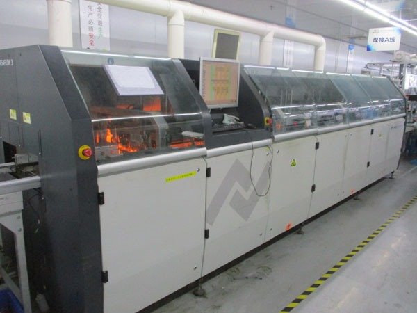
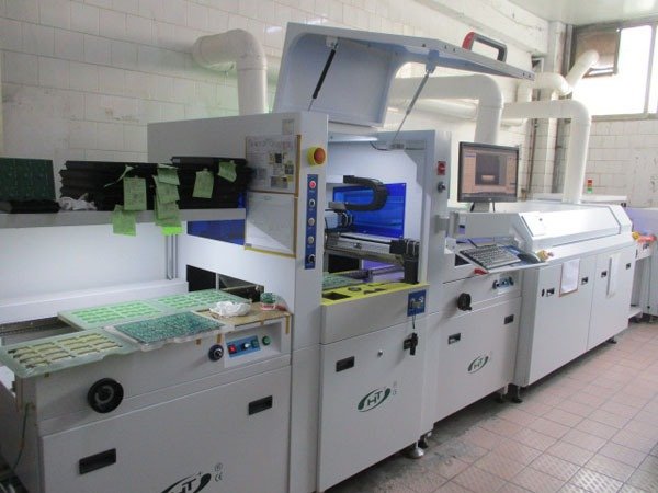
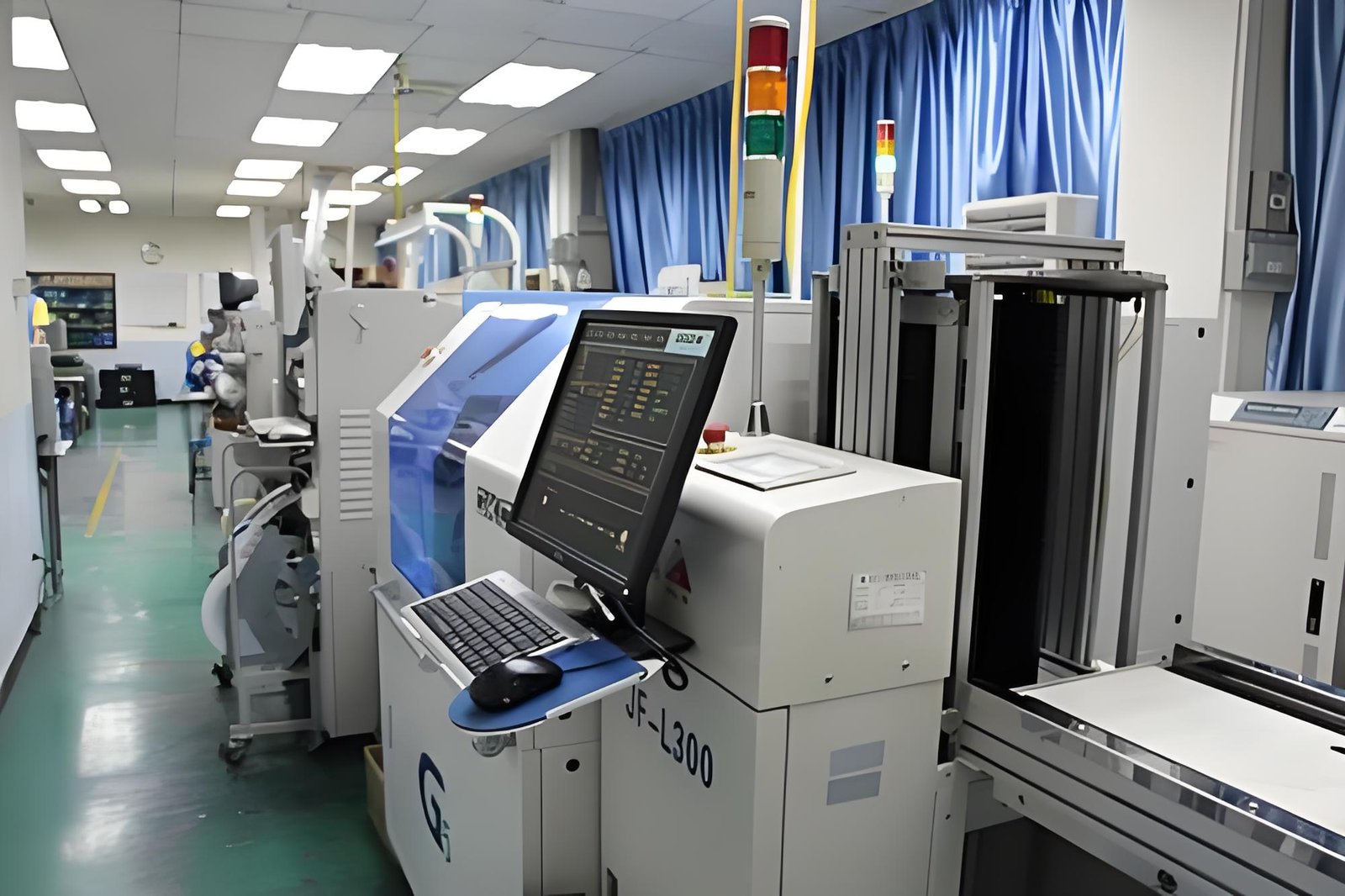
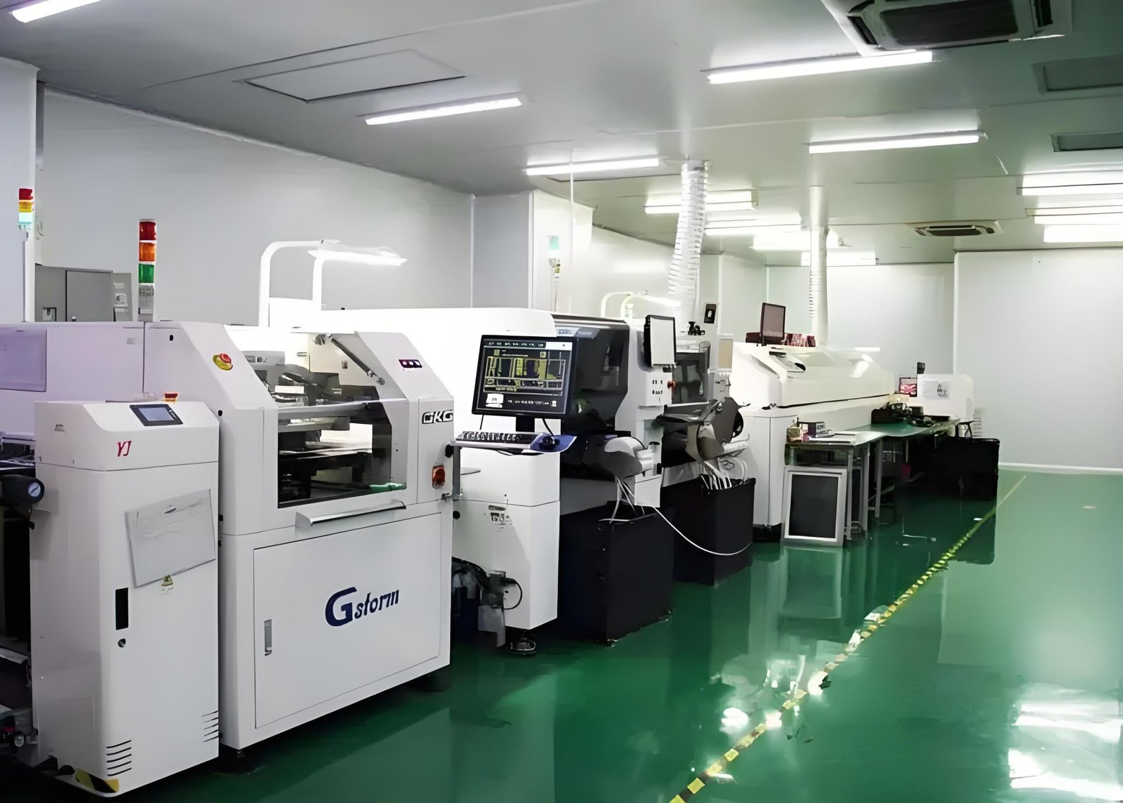
Our advanced equipment and skilled technicians ensure every assembly meets high standards of precision, durability, and consistency for demanding electronic applications.

We strictly follow international standards such as ISO 9001 and RoHS to ensure your PCBA products are compliant, audit-ready, and suitable for global market requirements.

From material handling to final inspection, we maintain tight process control using MES, AOI, and SPC tools—ensuring traceability, consistency, and zero-defect production.

Our production assembly services are designed to meet the unique challenges of the electronics industry. From small-batch runs of specialized components to large-scale production of critical devices, our skilled team ensures efficiency, consistency, and compliance with industry standards.
What Sets Our Production Assembly Apart?
Partner with us to keep your production process running smoothly and your customers satisfied.
| Quality Control Aspect | Description | Key Benefits |
|---|---|---|
| Incoming Material Inspection | All raw materials are thoroughly inspected before production to ensure they meet industry standards. | Ensures the highest quality foundation for PCBs. |
| Automated Optical Inspection (AOI) | Continuous monitoring of the production line with AOI to detect defects in the soldering process and component placement. | Maximizes accuracy, minimizes defects, and increases production efficiency. |
| X-ray Inspection | X-ray inspection is used to inspect internal connections and detect hidden soldering or assembly defects. | Detects hidden defects and ensures the reliability of multi-layer PCBs. |
| Functional Testing | Comprehensive testing of all functional aspects of the PCBs, including electrical performance and signal integrity. | Ensures that the final product performs to specifications and guarantees reliability. |
| Environmental Stress Testing | PCBs undergo tests under extreme temperature, humidity, and vibration conditions to simulate real-world stresses. | Verifies PCB durability under challenging conditions, such as in aerospace and military applications. |
| Final Visual Inspection | A detailed final inspection by experts ensures that all PCBs meet the strictest standards before shipping. | Prevents any cosmetic or minor defects from reaching the customer. |
| Statistical Process Control (SPC) | Utilizes data-driven analysis to monitor and control the production process for consistency. | Ensures ongoing consistency and high-quality output throughout production. |
We conduct a full range of quality tests including:
Solder Paste Inspection minimizing SMT board failures due to poor solder paste release.
Inspection Function:
It verifies the correct solder paste deposits for volume, area, height, offset and deformity to reduce solder joint defects.

We use lastest 3D AOI which had much better ability than 2D/2.5D AOI to see the defect of components after SMT & THT.
Inspection Function:
open and short circuits, wrong polarity of components, misplaced or missing components, wrong orientation of IC packages, stains, cuts, scratches, insufficient solder paste, solder bridges, cracked solder joints, excess solder etc.
X-ray inspection inspects inside the board and inside all components on the board verifying all connections have been made accurately.
Inspection Function:
Open circuit, short circuit, defective or fault connection,welding line offset bridging,Solder joints empty inspection and measurement,Integrity inspection of solder ball in array package and chip covering packaging.
before bulky production, we fabricate 5 pieces of PCBA first and randomly choose one piece for the FAI inspection.
If any issues arise during assembly, our FAI process will allow us to adjust our manufacturing equipment accordingly. After passing all quality checks, we will provide an FAI report for you to review and approve for bulky PCBA fabrication.
Functional testing imitate the real operating environment to verify their compliance with the design specification. It can also confirm the product performs in its intended environment.

Ensured stability and uniformity from the first board to full-scale production through automated lines and multi-stage process monitoring systems.
Our fully automated production lines ensure every PCBA—from prototypes to full-volume orders—meets the highest standards of quality and performance. With strict process control, standardized workflows, and real-time monitoring, we eliminate variability at every step.
Each board undergoes consistent placement, soldering, and inspection procedures, from SMT and reflow soldering to AOI and functional testing. This guarantees repeatability and accuracy, reducing common issues like prototype-pass but batch-fail scenarios and unstable solder quality.
Our scalable production system handles orders of any size without compromising consistency, improving delivery reliability and maintaining product integrity.


We ensure every PCB is defect-free with 100% electrical testing and Automated Optical Inspection (AOI) before shipment. Electrical testing uses flying probe testers and custom fixtures, checking critical parameters like continuity and impedance.
Our AOI systems detect micro-level defects like solder bridges and misalignment, ensuring quality at every stage of production. This thorough inspection process prevents errors and ensures reliable performance.
With over 40 years experience in the industry. We know a thing or two about PCBA manufacturing.
If you can’t find what you are looking for, please don’t hesitate to get in touch directly.
Simply fill in the form and we will try to get back to you ASAP. Alternatively, you can call or email us on the details below.

long@custompcba.com
+86-13023656973
Shenzhen Bao'an District, Xixiang Street, High-tech Center
long@custompcba.com

Automated page speed optimizations for fast site performance