
Printed Circuit Board Assembly (PCBA) is at the heart of modern electronics—but what exactly is it, and why is it so critical to understand?
PCBA refers to the process of mounting and soldering components onto a bare PCB to create a fully functional circuit board. It’s essential for everything from consumer electronics to industrial machinery.
From your smartphone and laptop to complex aerospace systems, almost every modern electronic device relies on at least one assembled circuit board. Behind each of these boards is a precise, step-by-step process that transforms a raw, copper-lined sheet into a working system.
Understanding how PCBA works—whether you’re a designer, product manager, or hobbyist—helps you make better decisions about design, cost, manufacturing, and testing. In this article, I’ll walk you through the essentials of PCBA: how it works, what’s involved, and why it’s the foundation of nearly every piece of tech you touch.
What Is PCBA?
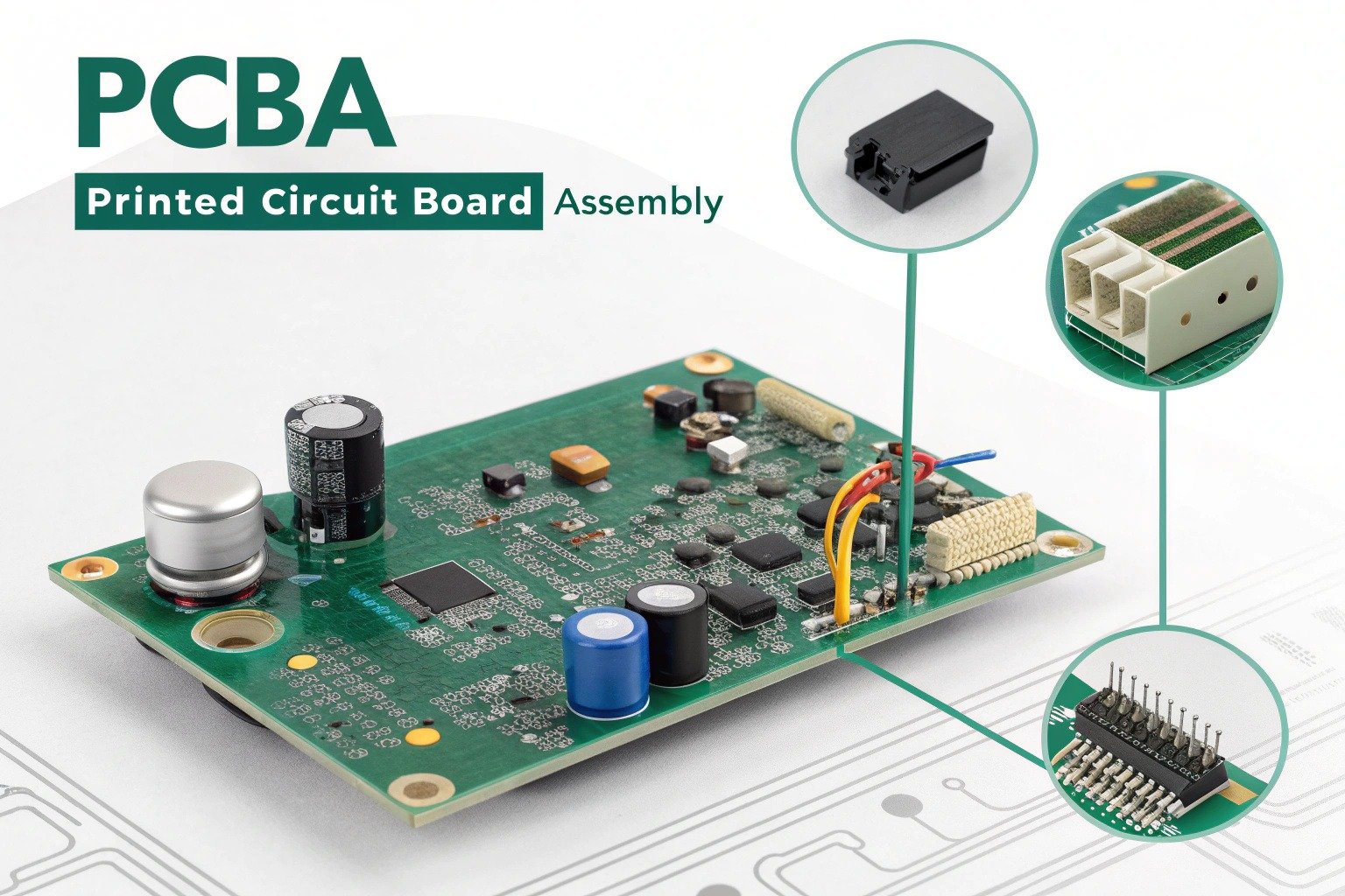
PCBA stands for Printed Circuit Board Assembly, which refers to the full process of soldering or mounting components like resistors, capacitors, ICs, and connectors onto a bare circuit board (PCB). The PCB itself only contains copper traces and drilled holes—it’s the skeleton. PCBA is what breathes life into it.
Once components are mounted and soldered, the board becomes a functional module capable of performing a specific task—whether that’s processing data, lighting an LED, or controlling a motor.
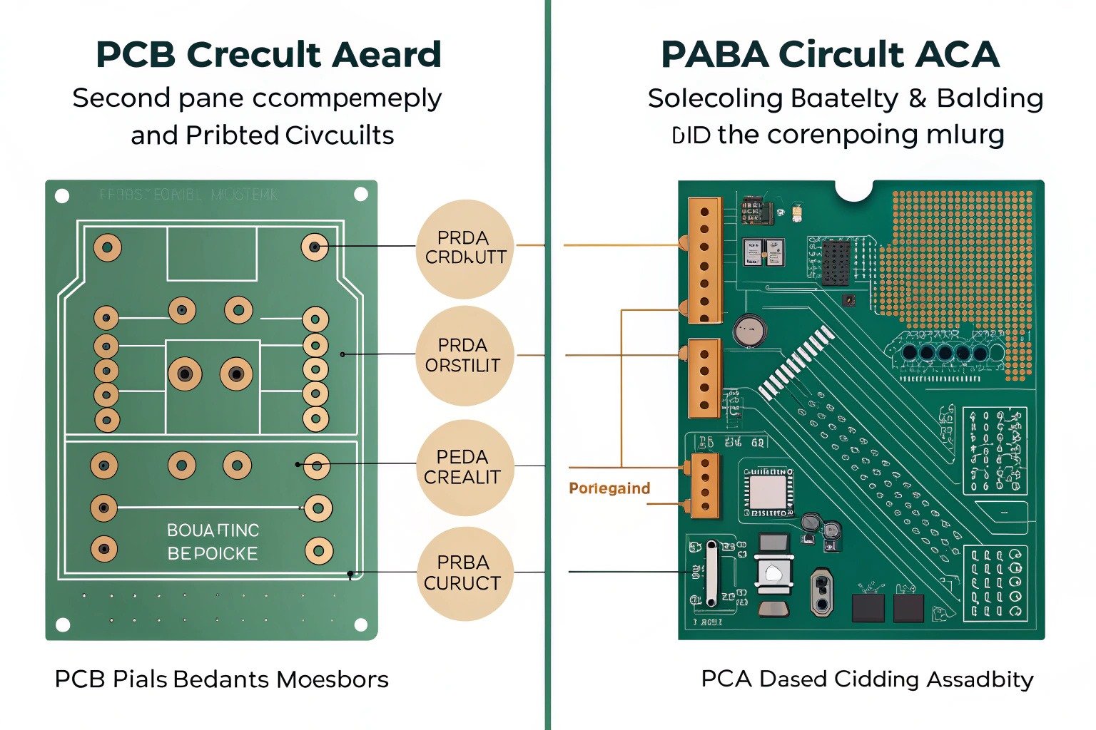
It’s important to distinguish between PCB (just the board) and PCBA (the finished board with all parts). This distinction matters when sourcing parts, preparing files, or communicating with manufacturers.
If you want to see real-world examples, JLCPCB provides a clear visual breakdown between bare PCBs and assembled PCBA products.
How PCBA Works
The PCBA process is usually automated, especially for high-volume production. But at its core, it involves a few critical steps:
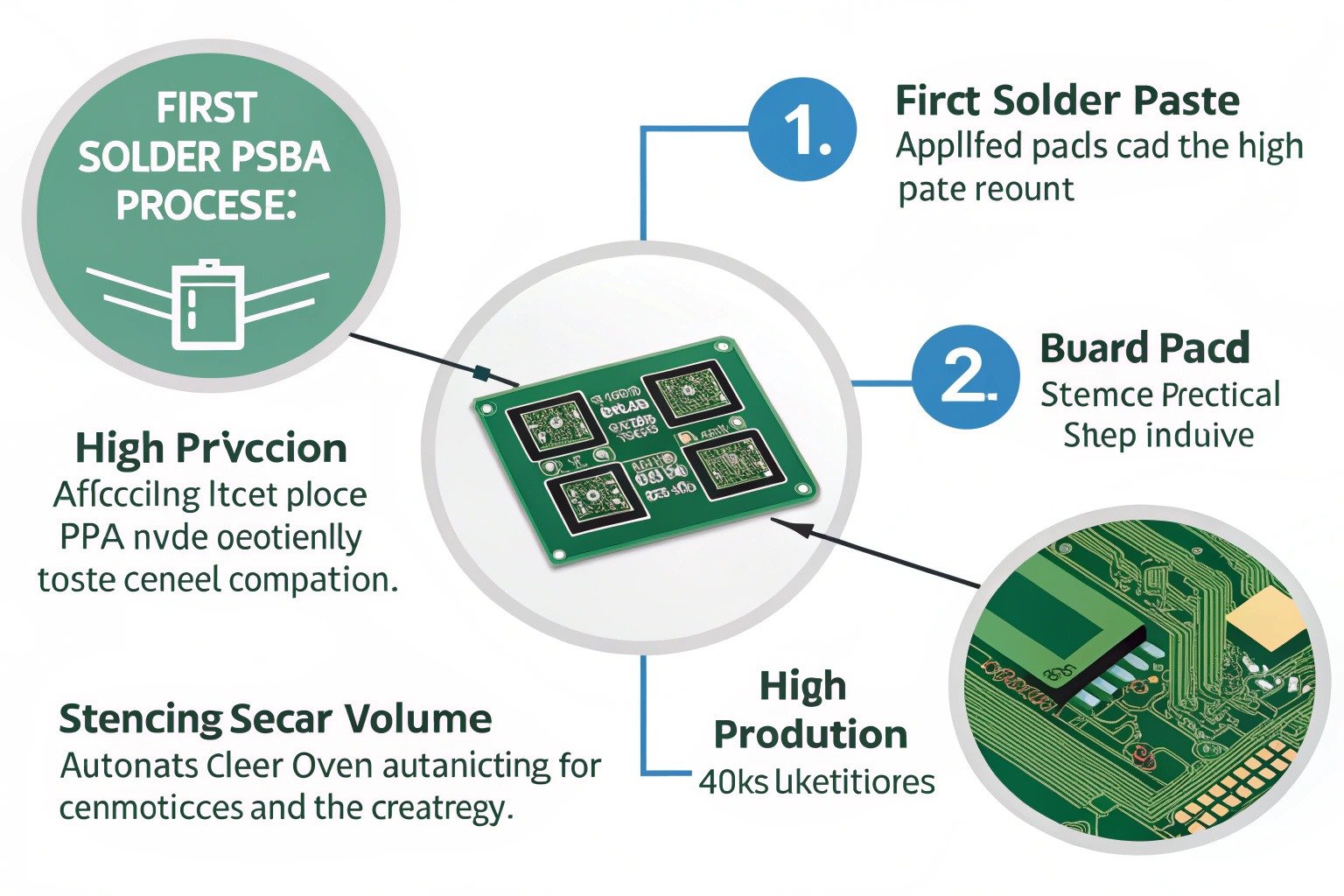
First, solder paste is applied to the board’s pads using a stencil. This paste holds components in place and contains the solder needed for bonding. After that, pick-and-place machines carefully mount each tiny component—sometimes placing thousands per hour.
Next comes reflow soldering, where the entire board is passed through a specialized oven. The heat melts the solder paste and permanently connects the components to the board.
After soldering, the board isn’t ready to go just yet. It must be inspected and tested to catch errors like solder bridges, missing parts, or misaligned chips. Advanced factories use AOI (Automated Optical Inspection) or even X-ray systems to ensure every joint is solid and clean.
For boards with through-hole parts, a second process called wave soldering may be used—or in some cases, skilled technicians solder them manually.
Types of PCBA Technologies
There are two main types of component mounting techniques used in PCBA, and each serves a different purpose.
-
SMT (Surface Mount Technology) is the most common today. Components are placed directly onto the surface of the board without needing holes. This allows for smaller, faster, and denser boards.
-
THT (Through-Hole Technology) is older but still relevant. Components have long leads that pass through drilled holes. It’s used for parts that need stronger mechanical support, like connectors or heavy transformers.
Most modern boards use a hybrid of SMT and THT, depending on what components are needed.
Want a visual comparison? Tempo Automation explains the differences here with examples and manufacturing considerations.
Why PCBA Quality Matters
A PCBA board is only as good as its weakest solder joint. Poor assembly leads to faulty connections, overheating, and early failure. That’s why quality control is baked into every step of the process—from material inspection to in-circuit testing (ICT).
If your PCBA has even one misaligned BGA or a cold solder joint, it can cause hard-to-trace bugs or complete failure in the field. And when you’re building at scale, a small mistake gets multiplied—costing time, money, and reputation.
Investing in reliable assembly partners, verified BOM sourcing, and clear design files pays off big time. It also helps avoid issues like counterfeit components, incorrect footprints, or poor thermal performance.
What to Look for in a PCBA Partner
If you’re outsourcing PCBA, your choice of partner matters. Look for a manufacturer who offers:
- Turnkey service (from PCB fabrication to assembly and testing)
- Transparent communication and fast DFM feedback
- IPC-certified quality and inspection processes
- Component sourcing through trusted distributors
- Support for low-volume prototypes as well as mass production
Before you commit, ask for a few sample builds or visit the factory if possible. Many top-tier suppliers, like Seeed Fusion, even provide online quoting tools and BOM validation.
Conclusion
PCBA is the critical process that transforms a bare board into a working, functional device. Whether you’re building a single prototype or manufacturing thousands of units, understanding the PCBA process helps you make smarter decisions in design, sourcing, and assembly.
By learning what’s involved—from solder paste and reflow ovens to testing and inspection—you can collaborate more effectively with engineers and manufacturers. And the better your board is assembled, the better your product will perform in the real world.
