
When I review customer projects, I always notice that successful PCB layouts start from one place: a clean, well-structured schematic. Good schematics reduce mistakes, improve communication, and prevent costly redesigns during PCB layout and assembly.
Schematic design rules define how to structure, label, and connect components clearly so the PCB layout is accurate, manufacturable, and easy to debug.
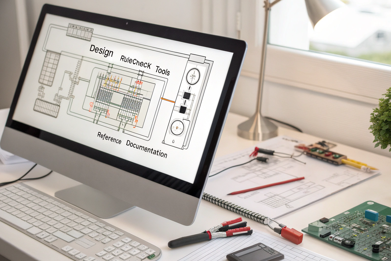
A well-designed schematic is more than lines and symbols—it’s the blueprint your entire product depends on. Let’s walk through the essential rules that keep your design stable from concept to production.
What are schematic design rules?
Over the years, I’ve seen many schematics that “look fine” but cause unexpected layout complications. The root issue is usually missing structure or unclear signals.
Schematic design rules are guidelines for organizing symbols, naming nets, defining connections, and presenting circuit logic clearly to avoid errors during PCB layout and manufacturing.

Why these rules matter in real hardware projects
A schematic guides every later step:
- PCB layout
- Component sourcing
- Assembly
- Testing
- Debugging
If the schematic has unclear nets or wrong footprints, the entire build is affected.
To avoid this, engineers follow rules that ensure:
| Rule Category | Purpose |
|---|---|
| Naming rules | Identify nets clearly |
| Symbol rules | Use correct part representations |
| Electrical rules | Prevent shorts, missing connections |
| Documentation rules | Help assembly and testing |
| DFM/DFT rules | Improve manufacturability and testability |
In my factory’s DFM checks, about 60% of early issues come from schematic mistakes. Once corrected, the PCBA stage becomes much smoother.
What schematic design rules should every engineer follow?
Through many years of working with hardware teams, I’ve collected a set of core rules that consistently prevent problems and improve clarity.
Key schematic design rules include clear net naming, correct symbol usage, organized page structure, proper power distribution, consistent reference designators, and full documentation.

A detailed breakdown of the essential rules
1. Use clear and consistent net names
Avoid cryptic or auto-generated names.
Good examples:
3V3_MAINI2C_SCLMCU_TX1SENSOR_PWR
Bad examples:
N00123TX?VCC_SOMETHING
Clear net names prevent wiring confusion during layout.
2. Group circuits into functional blocks
Organize pages by function:
- Power section
- MCU section
- Sensor section
- Communication interfaces
- Drivers and outputs
This helps both designers and technicians understand your circuit instantly.
3. Use correct and verified symbols + footprints
One of the biggest sources of PCBA errors is mismatched symbols and footprints.
Always verify:
- Pin order
- Pad size
- Package type (QFN, SOIC, BGA…)
- Polarity marks
My team often catches mismatched footprints during DFM reviews—fixing them early avoids expensive rework.
4. Define power rails clearly and consistently
Use global labels for power nets:
3V35V_USBVBATGND
And ensure:
- decoupling capacitors are placed near IC pins in the schematic
- power flow is visually clear
- separate analog/digital grounds if needed
This makes your layout and power integrity far more predictable.
5. Add decoupling capacitors to every major IC
A common beginner mistake is forgetting or placing decouplers far away in the schematic.
Each capacitor must be:
- placed next to the IC in the schematic
- correctly sized (0.1 µF, 1 µF, 10 µF…)
- connected to the correct pins
This helps the layout engineer place them correctly on the board.
6. Label component values and tolerances
Don’t leave fields blank.
Always include:
- resistor values
- capacitor values + voltage rating
- inductor values
- diode type
- IC part numbers
Clear values minimize sourcing and assembly mistakes.
7. Document test points and critical signals
Add test points for:
- power rails
- communication lines
- reset pins
- clock/test signals
This helps flying probe testing, FCT, and field debugging.
My factory routinely adds test recommendations when needed.
8. Avoid schematic “spaghetti wiring”
Use:
- net labels instead of long lines
- buses for grouped signals
- clear signal flow left → right
- neat wire routing
A clean schematic reduces misunderstandings and improves communication across teams.
9. Include notes, warnings, and design references
Good documentation prevents mistakes during layout and assembly.
Examples:
- “Use 2 oz copper for motor driver nets”
- “Keep this node away from noisy signals”
- “Match length within 5 mm”
- “This circuit requires isolated ground”
Technicians appreciate clear notes—they save time and avoid defects.
10. Run ERC (Electrical Rule Check) before releasing the file
Always fix:
- unconnected pins
- missing power pins
- duplicated references
- inconsistent net names
This step alone catches most simple mistakes.
How do schematic rules improve PCB manufacturing and assembly?
When customers ask why schematic discipline matters so much, I explain that the schematic directly affects everything downstream.
Following schematic rules improves manufacturability, reduces PCB errors, prevents assembly mistakes, and shortens debugging time during prototype and production builds.

Why schematic discipline matters from prototype to production
1. Better BOM accuracy
Clear part numbers prevent sourcing delays.
2. More predictable PCB layout
Good schematics naturally lead to good placement and routing.
3. Higher assembly yield
Correct footprints and clear decoupling prevent solder defects.
4. Easier testing
Documented test points accelerate FCT and flying probe testing.
5. Simpler debugging
When issues appear, everyone can read the schematic easily.
6. Fewer redesign cycles
Good schematic design reduces back-and-forth during DFM and layout review.
I’ve seen projects cut development time by 30–40% simply because their schematics were structured well.

Conclusion
Strong schematic design rules create the foundation of a stable, manufacturable, and easy-to-debug electronic product. By organizing your circuits, naming nets clearly, verifying symbols and footprints, and documenting important details, you make downstream PCB layout and assembly far smoother. With thoughtful planning and careful engineering practice, your schematic becomes a powerful blueprint that guides your product from concept to reliable production.
