
PCB testing methods are essential quality control tools used to verify electrical performance, assembly accuracy, and long-term reliability. In professional manufacturing, testing is integrated throughout the production flow to detect defects early and ensure stable performance before assembly and shipment.
In factory environments, PCB testing is not a single step but a system combining electrical, optical, and functional verification. The following seven PCB testing methods are the most widely used across modern manufacturing workshops.
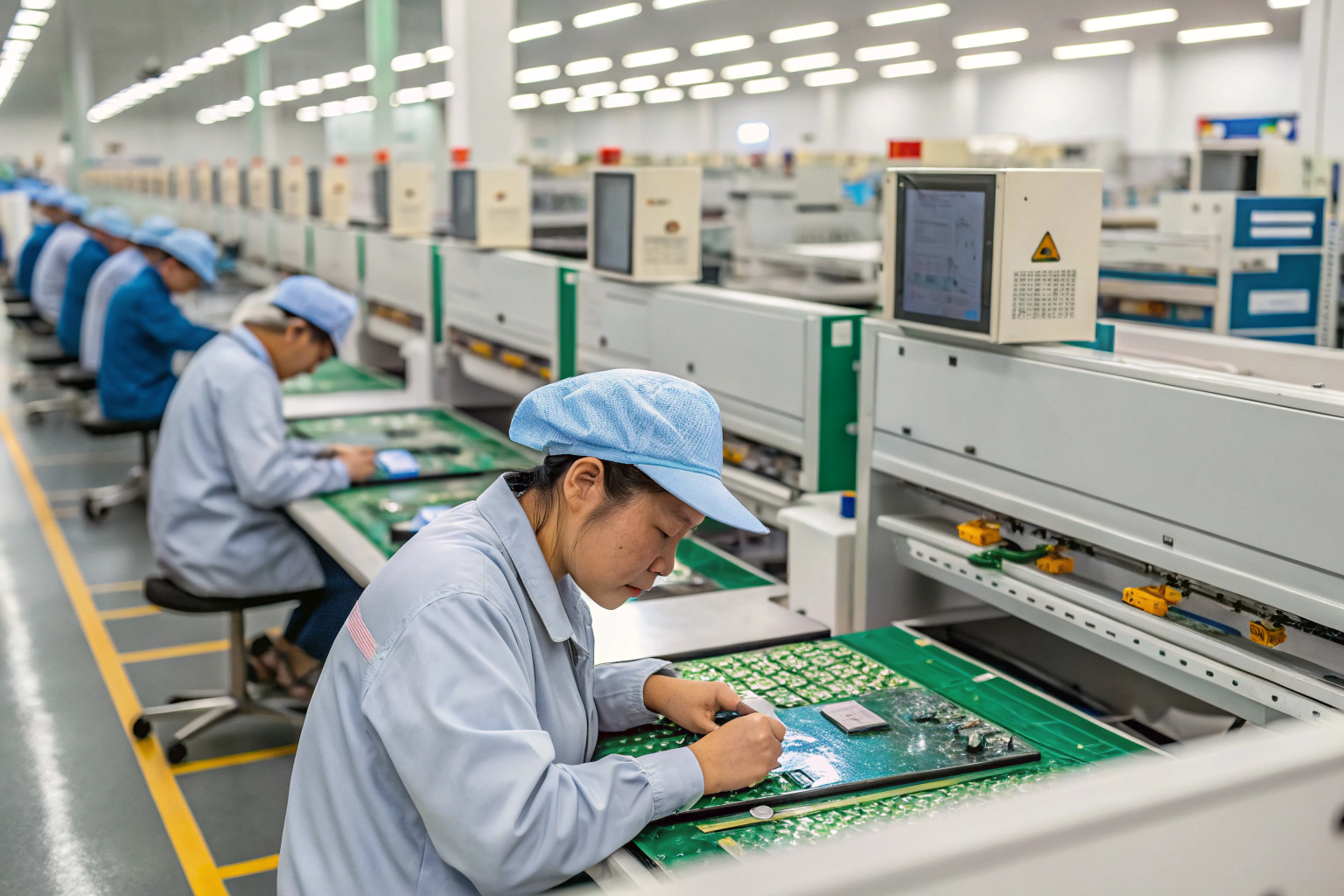
Visual Inspection (VI)
Visual inspection is the most basic PCB testing method and the first line of quality control.
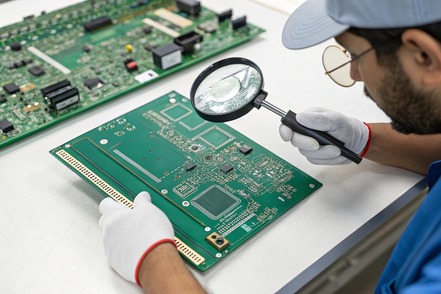
Operators or inspectors examine the PCB surface to identify visible defects such as scratches, broken traces, contamination, solder mask issues, or misprinted silkscreen markings.
In manufacturing workshops, visual inspection is often performed after key processes such as etching, solder mask application, and surface finishing. While it cannot detect electrical defects, it helps catch obvious process errors before boards move to the next stage.
Automated Optical Inspection (AOI)
AOI uses high-resolution cameras and image-processing software to inspect PCB features automatically.
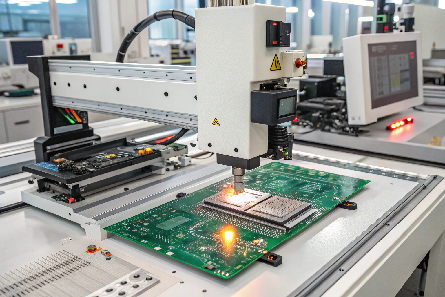
This method checks trace width, spacing, pad condition, solder mask alignment, and surface defects. AOI is faster and more consistent than manual inspection.
In factory production lines, AOI is commonly installed after imaging and etching, and again after assembly processes. It plays a key role in reducing human error and improving yield, especially for fine-line and high-density boards.
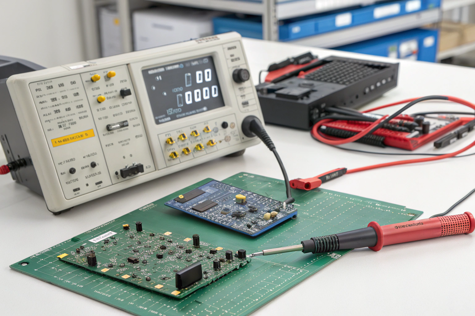
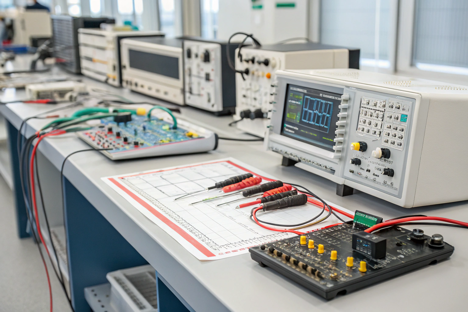
Electrical Testing (Continuity and Isolation Test)
Electrical testing verifies that all intended connections are present and that no unintended shorts exist.
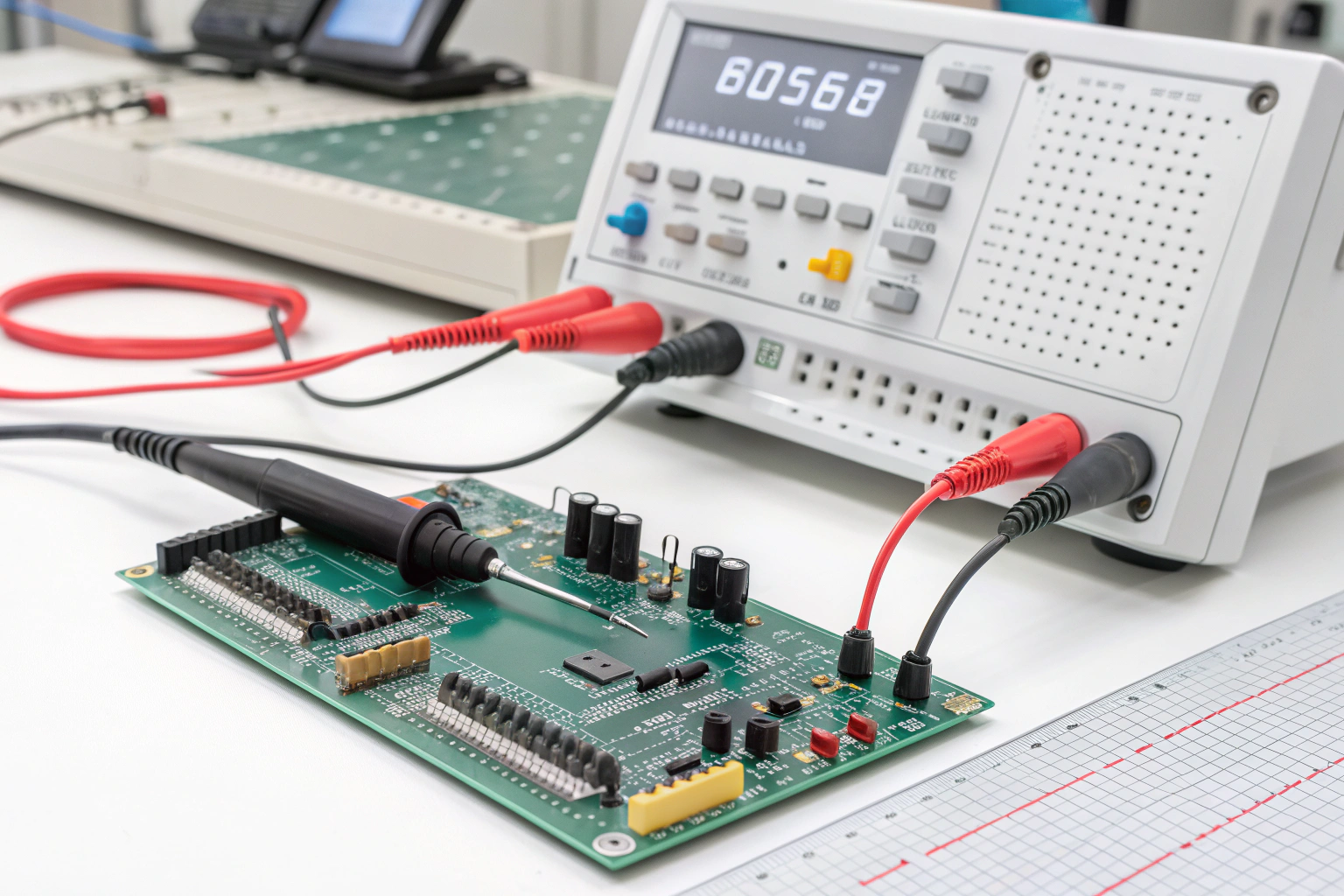
Using test fixtures or flying probe systems, the PCB is checked for continuity (open circuits) and isolation (short circuits) between nets.
This test is mandatory in PCB manufacturing. It ensures that the board meets its electrical design intent before assembly. For multilayer boards, electrical testing is especially critical to detect hidden inner-layer defects.
Flying Probe Testing
Flying probe testing is a flexible electrical testing method that does not require custom fixtures.
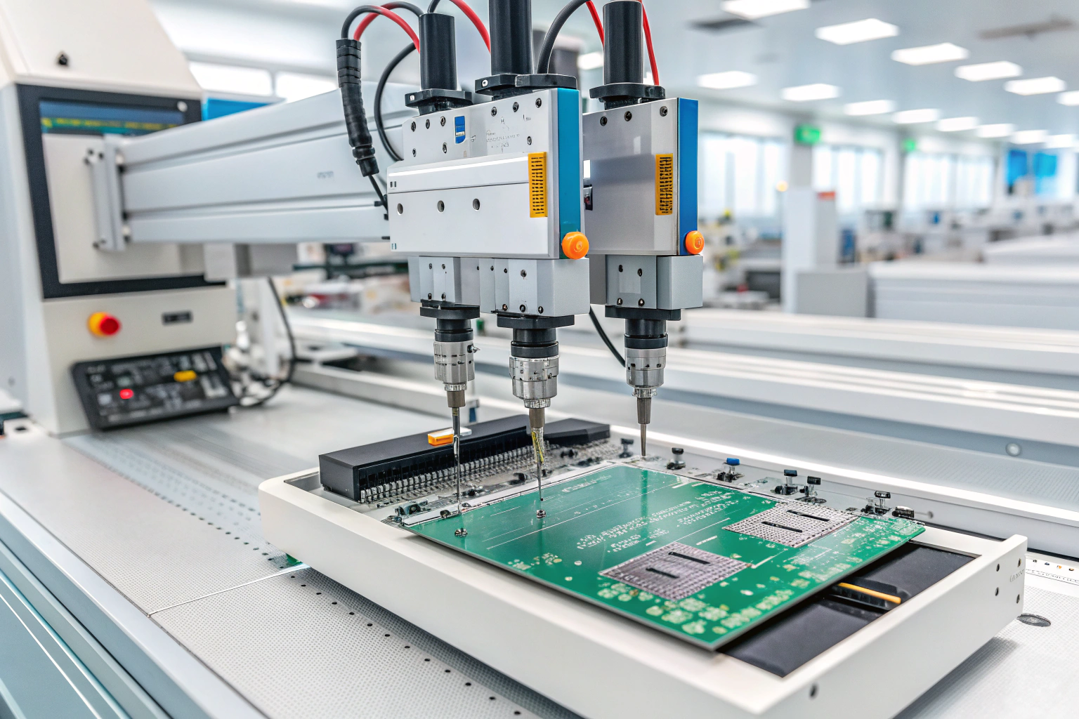
Movable probes contact test points directly according to programmed coordinates. This method is ideal for prototypes and low-volume production.
In factory settings, flying probe testers are widely used for quick-turn boards and design verification. Although slower than fixture-based testing, they reduce tooling cost and allow rapid design changes.
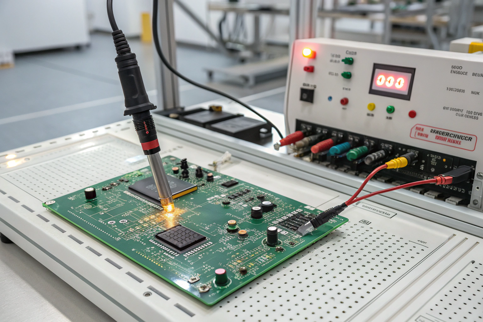
In-Circuit Testing (ICT)
ICT is used primarily after PCB assembly but is closely linked to bare board quality.
It checks component values, solder joint integrity, polarity, and basic circuit behavior by probing individual nodes on the assembled board.
From a manufacturing perspective, strong bare PCB quality improves ICT pass rates. Factories often coordinate PCB fabrication tolerances with assembly and test engineering to ensure stable probe contact and accurate results.
Functional Testing (FCT)
Functional testing verifies that the PCB operates as intended under real or simulated working conditions.
Power is applied, signals are transmitted, and outputs are measured to confirm correct behavior.
In manufacturing workflows, FCT is typically performed after assembly, but its effectiveness depends heavily on PCB fabrication quality. Stable impedance, reliable vias, and clean surfaces contribute to consistent functional performance.
X-Ray Inspection
X-ray inspection is used to examine hidden features that cannot be seen optically.
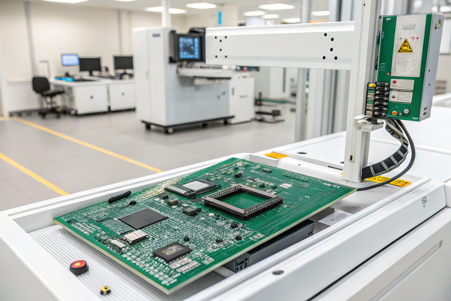
It is especially useful for multilayer PCBs and boards designed for fine-pitch components, where internal structures or buried features must be verified.
In manufacturing environments, X-ray inspection supports failure analysis and process validation. It helps engineers identify internal defects early and improve upstream fabrication control.
How do factories integrate PCB testing into production?
In professional PCB manufacturing, testing methods are distributed across different workshops.
Visual inspection and AOI are used during fabrication. Electrical testing confirms circuit integrity before shipment. Advanced methods such as X-ray and functional testing support complex or high-reliability products.
This layered testing approach prevents defective boards from moving forward and reduces downstream repair costs.
Conclusion
The seven main PCB testing methods—visual inspection, AOI, electrical testing, flying probe testing, ICT, functional testing, and X-ray inspection—form a complete quality assurance system in modern manufacturing.
Each method addresses different risk points, from visible defects to hidden electrical issues. When applied systematically across factory workshops, these testing methods ensure that PCBs deliver consistent electrical performance, strong reliability, and stable compatibility with assembly processes throughout their entire lifecycle.
