
As electronic products continue to evolve toward higher performance and greater integration, traditional single-layer or double-layer PCBs often struggle to meet electrical and manufacturing requirements. Multilayer PCBs have become a mainstream solution because they address these challenges in a structured and scalable way.
The advantages of multilayer PCBs include higher routing density, improved signal integrity, stable power distribution, better EMI control, reduced board size, and more reliable manufacturing performance.
These benefits make multilayer PCBs a core technology in modern electronics production.
The following sections explain the main advantages of multilayer PCBs from both an engineering and factory manufacturing perspective.
Higher Circuit Density and Design Flexibility
More layers create more routing space.
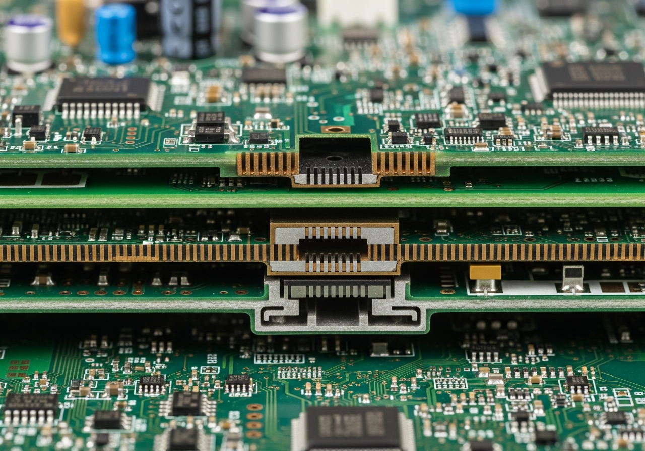
Multilayer PCBs provide additional internal copper layers that significantly increase routing capacity. Instead of forcing all signals, power, and ground onto surface layers, routing can be distributed across multiple internal planes.
This allows:
- Shorter and more direct signal paths
- Fewer routing compromises
- Better separation between different circuit functions
From a manufacturing standpoint, cleaner routing reduces trace congestion and spacing violations. This improves etching accuracy, lowers defect rates, and increases yield stability during volume production.
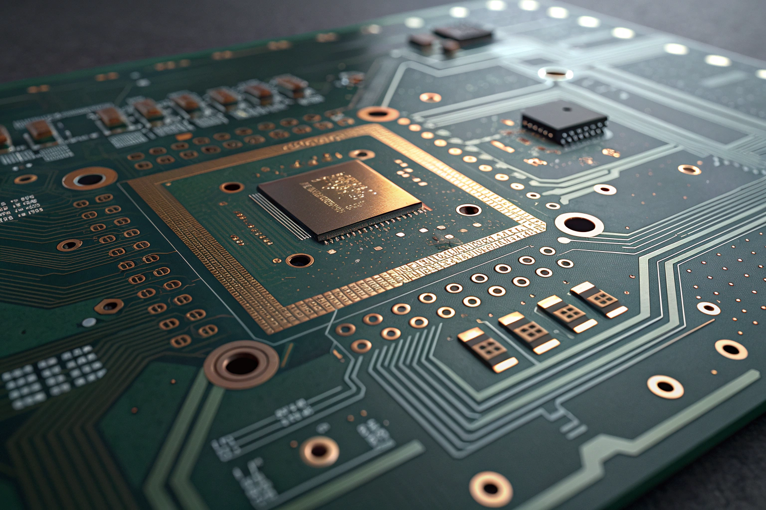
Improved Signal Integrity and Electrical Performance
Controlled signal behavior is a major advantage.
High-speed and sensitive signals are vulnerable to noise, impedance mismatch, and crosstalk when routed on crowded surface layers.
Multilayer PCBs allow signal layers to be placed next to continuous ground planes. This structure:
- Provides stable reference paths
- Enables controlled impedance
- Reduces signal reflection and crosstalk
In production environments, this results in more predictable electrical performance and fewer functional variations between different manufacturing batches.
Stable Power and Ground Distribution
Power quality improves with dedicated planes.
In complex circuits, distributing power through narrow traces leads to voltage drop and noise coupling.
Multilayer PCBs typically include solid power and ground planes that:
- Lower distribution impedance
- Improve current sharing
- Enhance decoupling capacitor effectiveness
- Reduce ground bounce and noise
During factory testing and aging processes, boards with solid planes show more stable behavior under dynamic load conditions, reducing intermittent failures.
Better EMI and EMC Performance
Noise control is built into the PCB structure.
Electromagnetic interference often originates from long signal loops and undefined return paths.
Ground planes inside multilayer PCBs act as shields that contain electromagnetic fields and isolate sensitive circuits from noisy ones. Layer separation also allows power circuits, digital signals, and analog sections to be placed on different layers.
This structural EMI control reduces the need for external shielding and helps products meet electromagnetic compatibility requirements more efficiently.
Smaller Board Size and Higher Integration
Functionality moves vertically instead of horizontally.
By adding internal routing layers, more circuitry can be placed within the same or smaller board outline.
This enables:
- Smaller enclosures
- Higher functional integration
- More compact product layouts
In manufacturing, smaller board sizes can improve panel utilization and reduce material waste, even when layer count increases. This often leads to better overall cost efficiency at the system level.
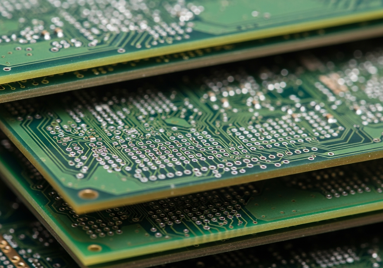
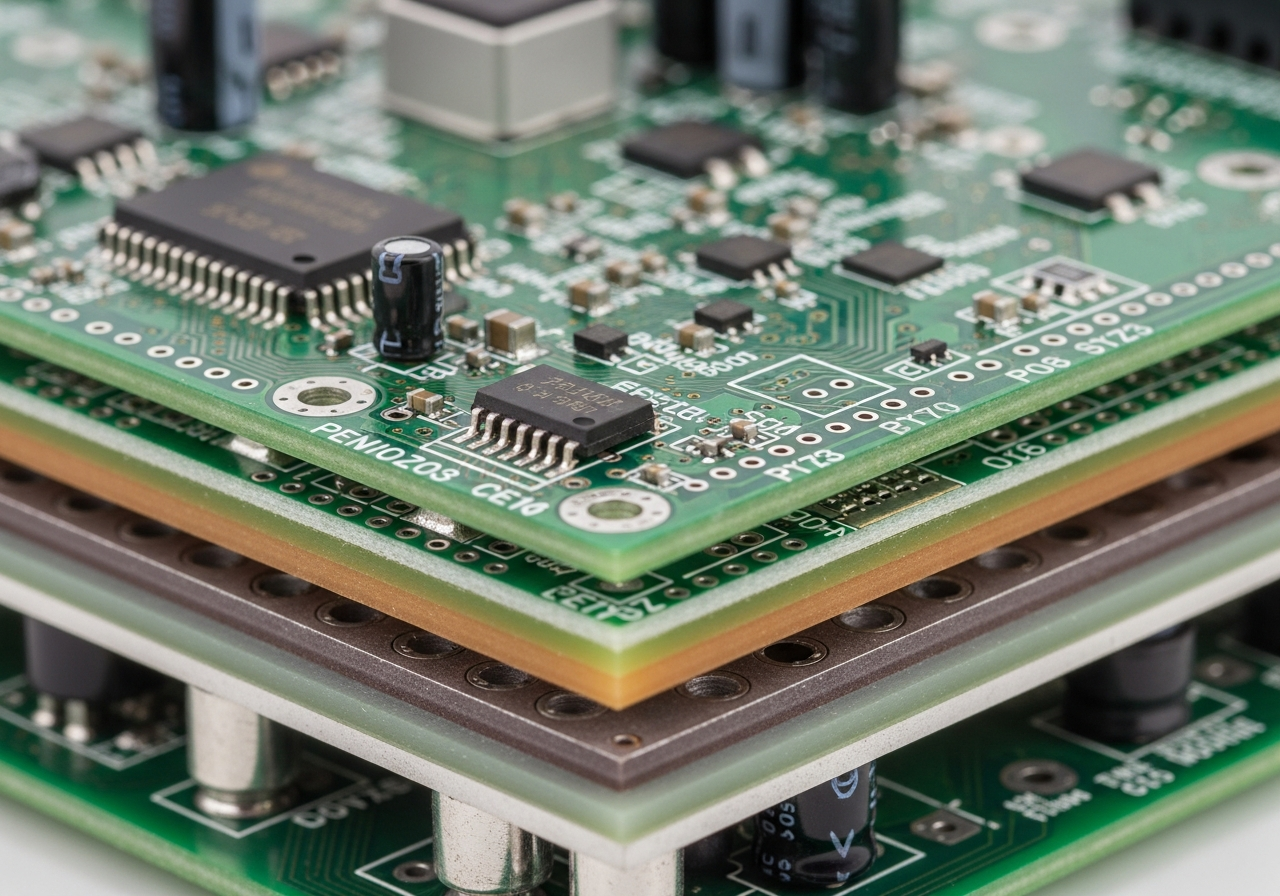
Better Manufacturing Stability and Assembly Reliability
Balanced structures improve process control.
Even-layer multilayer PCBs use symmetric stack-ups that distribute mechanical stress evenly.
In factory workshops, this leads to:
- Reduced board warpage during reflow soldering
- Improved coplanarity for fine-pitch components
- More consistent solder joint quality
- Higher AOI and functional test pass rates
Standard multilayer stack-ups also fall within mature process windows, making quality easier to control from pilot runs to full-scale production.
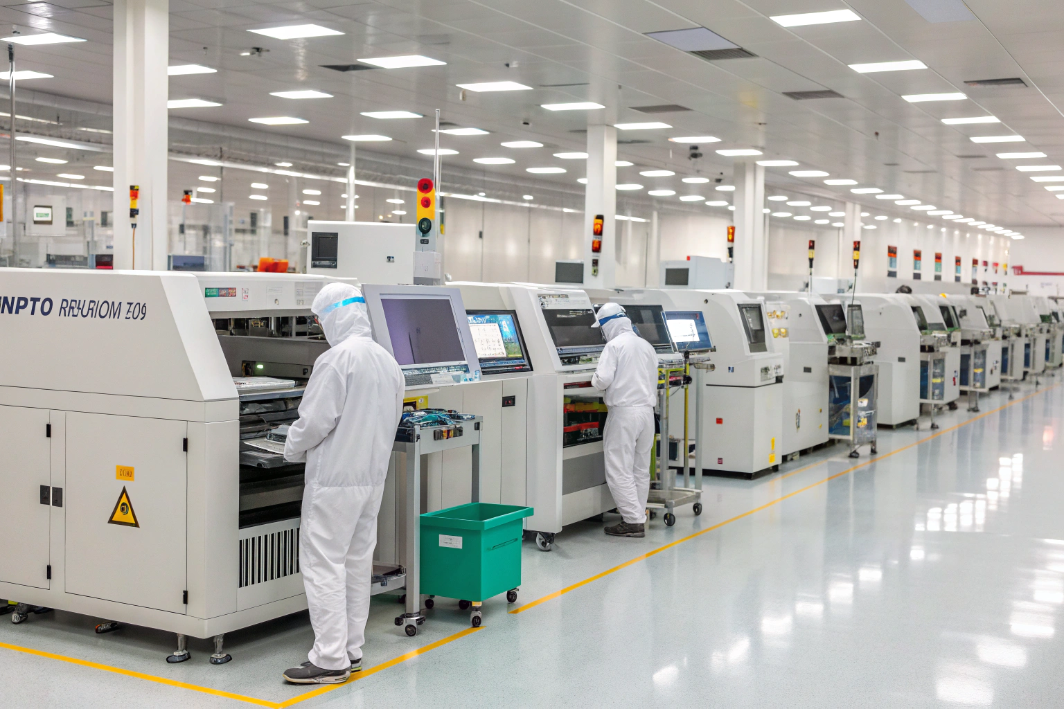
How Factory Processes Support Multilayer PCB Advantages
Process discipline ensures consistency.

Producing multilayer PCBs involves tightly controlled steps such as inner-layer imaging, lamination, drilling, plating, and inspection.
Key manufacturing controls include:
- Inner-layer AOI before lamination
- Precise stack-up and alignment control
- Stable lamination temperature and pressure
- Via plating thickness monitoring
- Electrical testing and final inspection
These controls ensure that internal layers perform as designed and remain reliable throughout the product lifecycle.
Conclusion
Multilayer PCBs offer significant advantages in routing capacity, signal integrity, power stability, EMI control, compact design, and manufacturing reliability. By distributing electrical functions across multiple internal layers, they create a structured and predictable electrical environment that single or double layer boards cannot easily achieve.
From a manufacturing perspective, multilayer PCBs also benefit from standardized stack-ups, mature lamination processes, and well-established inspection methods. These factors lead to higher assembly yield, more consistent quality, and stronger long-term reliability. As electronic products continue to demand higher performance and tighter integration, multilayer PCBs remain a fundamental and efficient solution for stable, scalable, and high-quality electronics manufacturing.
