
A multilayer PCB is a complex engineered structure made up of multiple functional materials and layers. Each component inside the board has a specific role, working together to support electrical performance, mechanical strength, thermal stability, and long-term reliability. Understanding these components is essential for proper design, manufacturing, and quality control of advanced electronic products.
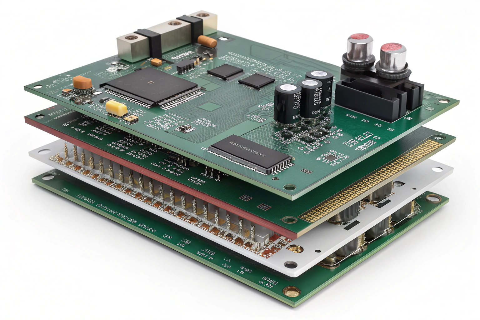
The main components of a multilayer PCB include copper layers, insulating dielectric materials, prepreg, vias, solder mask, surface finish, and silkscreen. These elements are laminated into a single structure that enables high-density routing, stable signal transmission, and reliable power distribution.
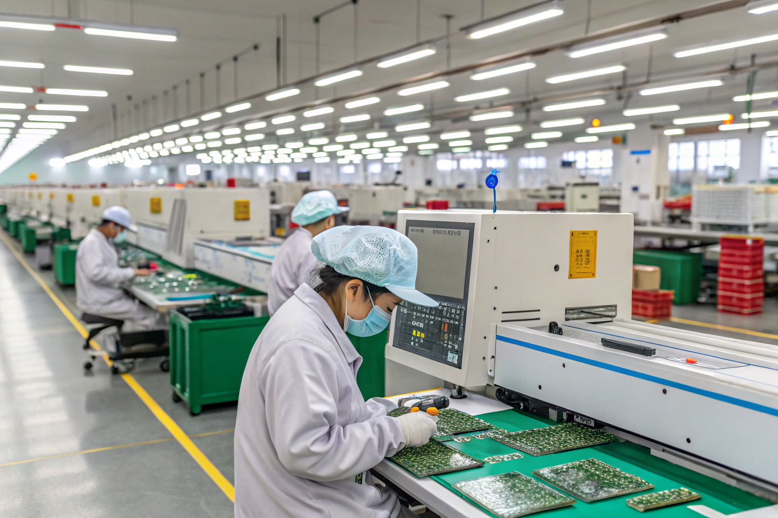
The following sections explain each major component in detail, from both an engineering and manufacturing perspective, with additional focus on factory processes and production control.
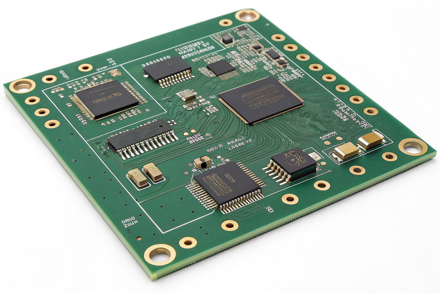
Copper Layers: The Electrical Backbone
Copper layers are the most critical functional components of a multilayer PCB. They form the conductive paths that carry electrical signals, power, and ground connections throughout the board.
In a multilayer PCB, copper layers are divided into:
- Signal layers for routing data and control signals
- Power layers for voltage distribution
- Ground layers for return paths and noise suppression
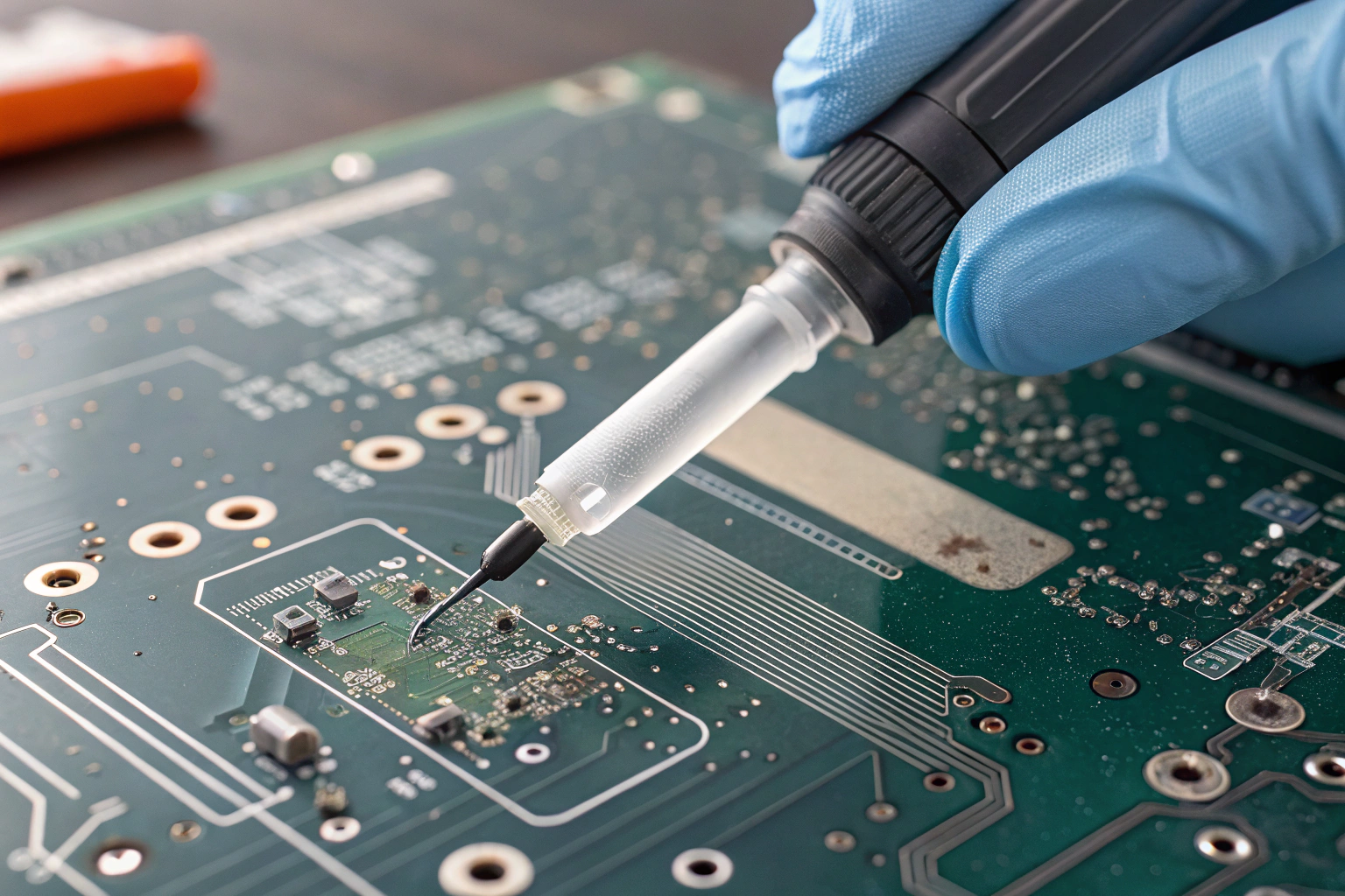
Copper thickness is carefully selected based on current requirements and thermal performance. Typical thickness ranges from 0.5 oz to 2 oz, with heavier copper used for power electronics. During manufacturing, inner copper layers are etched first and inspected before lamination to ensure trace accuracy. Any defect in inner copper layers becomes permanently trapped after lamination, so strict inspection is essential.
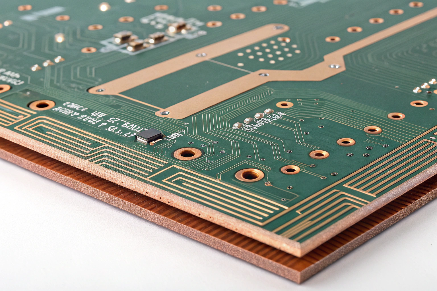
Core Material: Structural Support and Insulation
The core is a rigid dielectric material with copper bonded to one or both sides. It provides mechanical strength and electrical insulation between copper layers.
Common core materials include:
- Standard FR4 epoxy glass laminate
- High-Tg FR4 for improved thermal resistance
- Specialized laminates for high-frequency designs
The core thickness influences board rigidity and impedance control. In multilayer boards, multiple cores may be used depending on stack-up design. From a factory standpoint, core material quality affects drilling accuracy, lamination stability, and long-term reliability. Material certificates are usually verified before production to ensure consistency.
Prepreg: The Bonding Layer
Prepreg is a fiberglass material impregnated with partially cured resin. It plays a dual role in multilayer PCBs: electrical insulation and layer bonding.
During lamination, prepreg:
- Melts and flows under heat and pressure
- Bonds copper layers and cores together
- Fills gaps and creates a solid structure
Resin flow characteristics must be carefully matched to the stack-up design. Too much flow can cause resin starvation, while too little flow can create voids. In the factory, lamination parameters such as temperature, pressure, and time are tightly controlled to ensure uniform bonding and prevent delamination.
Vias: Vertical Electrical Connections
Vias are plated holes that connect copper layers vertically. They allow signals and power to travel between layers in a multilayer PCB.
Common via types include:
- Through-hole vias
- Blind vias
- Buried vias
Via reliability depends on drilling precision and copper plating quality. Poor via plating can lead to intermittent connections or failure under thermal stress. Manufacturing processes include controlled drilling, desmearing, and electroplating to ensure strong and uniform via walls. For high-reliability boards, via integrity is one of the most closely monitored parameters.
Dielectric Layers: Electrical Isolation and Signal Control
Dielectric layers separate copper layers and prevent electrical shorts. At the same time, they influence signal behavior, especially in high-speed designs.
Key dielectric properties include:
- Dielectric constant (Dk)
- Dissipation factor (Df)
- Thermal stability
The thickness of dielectric layers affects impedance and crosstalk. In multilayer PCBs, dielectric spacing is calculated during design and verified during production. Consistent dielectric thickness across the board ensures stable electrical performance and predictable signal behavior.
Solder Mask: Protection and Insulation
Solder mask is a protective coating applied to the outer copper layers. It prevents oxidation, protects traces from damage, and avoids solder bridging during assembly.
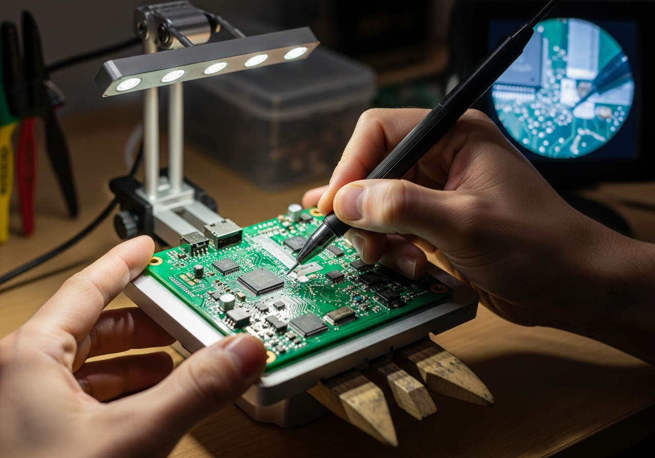
In multilayer PCBs, solder mask also improves surface insulation and environmental resistance. During manufacturing, solder mask alignment and thickness are carefully controlled. Poor solder mask quality can cause assembly defects or reduce board reliability in harsh environments.
Surface Finish: Ensuring Solderability
Surface finish is applied to exposed copper pads to protect them from oxidation and ensure reliable soldering during assembly.
Common surface finishes include:
- HASL (lead-free)
- ENIG
- OSP
- Immersion silver or tin
The choice of surface finish affects shelf life, solder joint quality, and compatibility with fine-pitch components. In production, surface finish thickness and uniformity are verified to prevent solder defects during SMT assembly.
Silkscreen: Identification and Assembly Guidance
Silkscreen is the printed layer that shows component outlines, reference designators, polarity marks, and other identifiers.
Although it does not affect electrical performance, silkscreen plays an important role during assembly, inspection, and maintenance. Clear and accurate markings reduce assembly errors and improve traceability in manufacturing environments.
Conclusion
A multilayer PCB is not a single material but a precisely engineered system composed of copper layers, core materials, prepreg, vias, dielectrics, solder mask, surface finish, and silkscreen. Each component contributes to the board’s electrical function, mechanical strength, and long-term reliability.
The interaction between these components is established during design and finalized during manufacturing. Inner layer accuracy, lamination quality, via plating, and surface protection all determine whether the final board can meet performance and durability requirements. As electronic systems continue to increase in complexity and density, the proper selection and control of multilayer PCB components becomes even more critical.
When each component is designed correctly and manufactured under strict process control, a multilayer PCB delivers stable signals, reliable power distribution, and consistent performance throughout its service life.
