
Printed circuit boards are commonly classified into three main types based on their structural complexity: single-layer PCBs, double-layer PCBs, and multilayer PCBs. Each type follows a different manufacturing process and is suited to different performance and reliability requirements.
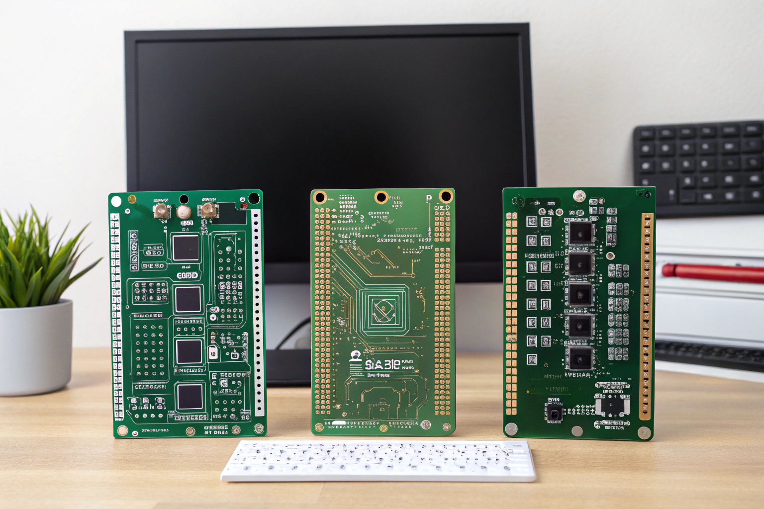
From a manufacturing perspective, these three PCB types represent increasing levels of process complexity, equipment demand, and quality control. Understanding their differences helps clarify why production flow, workshop layout, and process control vary significantly between them.
What is a single-layer PCB?
A single-layer PCB, also known as a single-sided PCB, has conductive copper traces on only one side of the board. All components are mounted on the same side, and there are no internal layers.

In factory production, single-layer PCBs have the simplest process flow. Manufacturing steps typically include material cutting, imaging, etching, drilling, solder mask application, surface finish, and electrical testing. No lamination is required.
Because of their simple structure, single-layer PCBs are easy to manufacture with high yield and stable quality. They are often used in basic control circuits, power supplies, and simple electronic products where circuit density and signal integrity demands are low.
How are double-layer PCBs different?
Double-layer PCBs have copper traces on both the top and bottom sides of the board. Electrical connections between layers are made using plated through holes.
Manufacturing double-layer PCBs introduces additional complexity compared to single-layer boards. Drilling accuracy and hole plating quality become critical, as vias must provide reliable electrical connections between layers.
In the factory, these boards require precise drilling, stable copper plating, and strict inspection of via integrity. Double-layer PCBs support higher routing density and better circuit flexibility, making them suitable for industrial controls, consumer electronics, and communication devices.
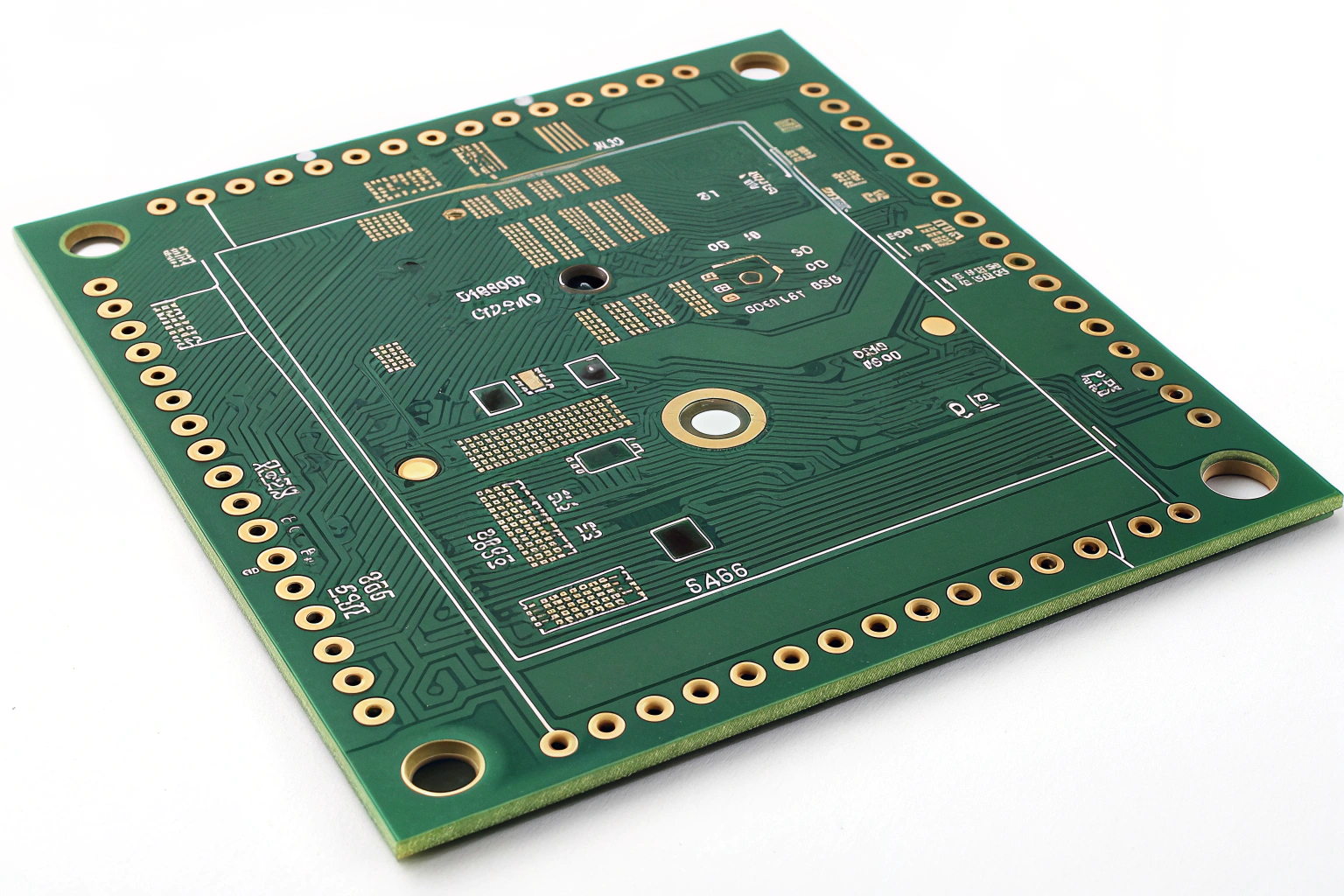
What defines a multilayer PCB?
A multilayer PCB contains three or more conductive copper layers stacked and laminated together. Common configurations include 4-layer, 6-layer, and higher layer counts.
From a manufacturing standpoint, multilayer PCBs represent the highest level of complexity. Production involves inner-layer imaging and etching, optical inspection, lamination under high temperature and pressure, precision drilling, plating, and outer-layer processing.
Internal power and ground planes improve signal integrity, noise control, and power distribution. This makes multilayer PCBs essential for high-speed, high-density, and high-reliability electronic systems.
How do factory workshops differ for each PCB type?
Each PCB type requires a different workshop focus.
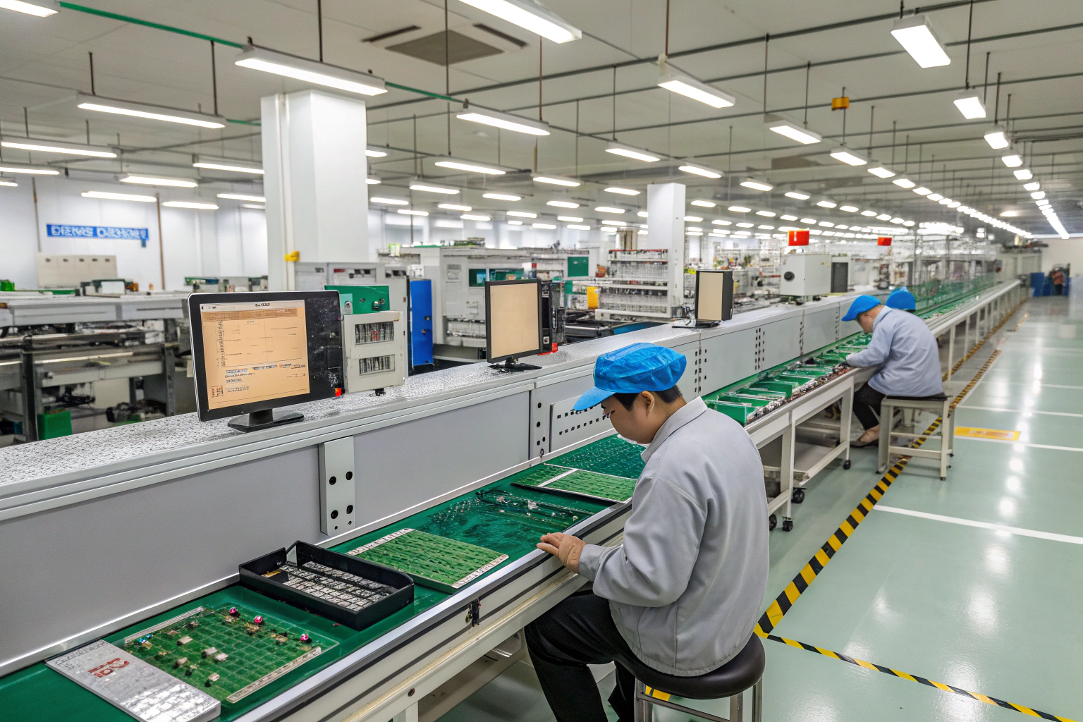
Single-layer and double-layer PCBs mainly rely on etching, drilling, and plating workshops. Multilayer PCBs require dedicated inner-layer processing areas, lamination presses, registration control systems, and advanced inspection equipment.
Factories producing all three types must carefully separate process flows to avoid cross-contamination and maintain efficiency. Multilayer production lines typically operate under tighter environmental and process controls to ensure layer alignment and material stability.
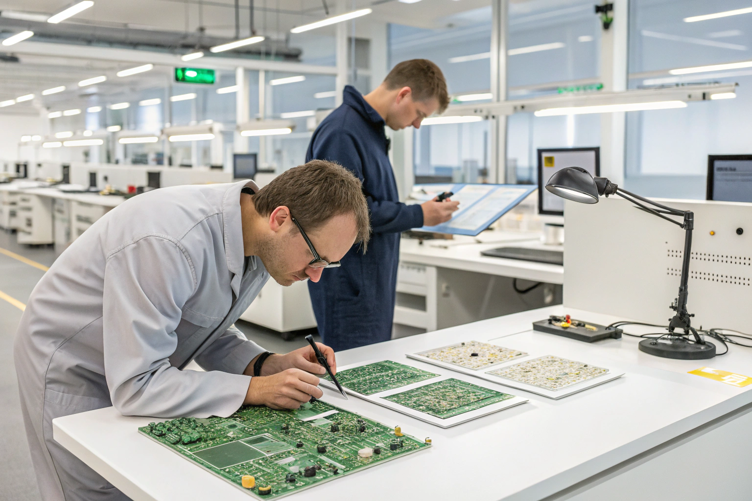
How does process control change with PCB complexity?
As PCB types progress from single-layer to multilayer, process control becomes increasingly critical.
For simple boards, visual inspection and basic electrical testing are often sufficient. For multilayer boards, automated optical inspection, layer registration checks, and controlled lamination profiles are essential.
Tighter trace width, smaller vias, and higher layer counts reduce process margins. Manufacturing discipline and engineering involvement increase accordingly to maintain yield and long-term reliability.
How are the three PCB types selected in production planning?
PCB type selection depends on electrical performance, mechanical requirements, and product lifecycle expectations.
Single-layer PCBs prioritize simplicity and cost efficiency. Double-layer PCBs balance routing flexibility and manufacturing effort. Multilayer PCBs focus on performance, stability, and compact design.
From a manufacturing view, early alignment between design intent and production capability reduces redesign cycles and improves delivery stability.
Conclusion
The three main types of PCBs—single-layer, double-layer, and multilayer—represent a clear progression in structure, performance, and manufacturing complexity. Each type requires a different production flow, level of process control, and factory capability.
As circuit demands increase, manufacturing shifts from simple etching-based processes to highly controlled lamination and multilayer production systems. Understanding these differences supports better design decisions, smoother production planning, and more reliable PCB performance across the entire product lifecycle.
