
A high grade circuit board looks clean, precise, consistent, and well-controlled, both visually and structurally. Quality is not defined by color or thickness alone, but by how well materials, layout, soldering, and manufacturing processes work together to deliver long-term reliability.
High grade PCBs are designed to perform predictably under heat, load, and time. Their quality is visible to trained eyes and measurable through inspection and testing.
In professional manufacturing, appearance is only the surface layer of quality. What matters more is what the board reveals about process discipline and engineering control.
Clean and Consistent Solder Joints Are the First Visual Signal
Solder joints reveal manufacturing quality instantly.
They are the most honest indicator.
On a high grade circuit board, solder joints are:
- Smooth and evenly shaped
- Properly wetted to pads and leads
- Consistent across the entire board
- Free of cracks, spikes, or solder balls
The surface may appear shiny or matte depending on alloy type, but consistency is key. Uneven joints, excess solder, or dull grainy surfaces suggest unstable thermal control or poor process discipline.
In factory workshops, this level of solder quality is achieved through:
- Verified reflow profiles
- Stable solder paste printing
- Controlled cooling rates
- Strict inspection standards
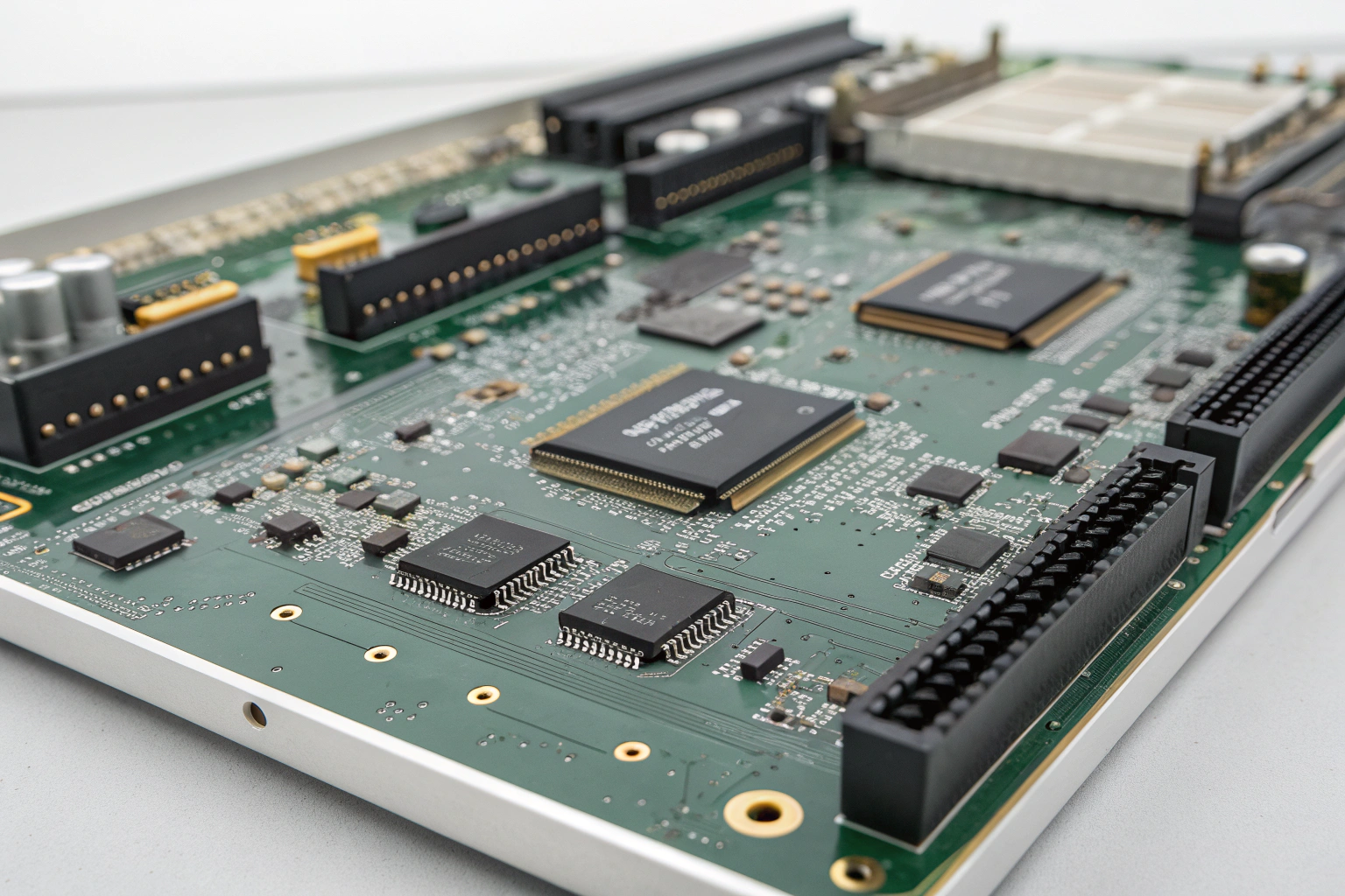
High grade boards show uniform solder quality not just on one component, but on every component, including fine-pitch and large thermal parts.
Precise Component Placement and Alignment
Alignment reflects both equipment accuracy and process control.
Misalignment is never random.
High grade circuit boards show:
- Perfectly centered components on pads
- Correct orientation and polarity
- Even spacing between parts
- No tilted, skewed, or floating components
Fine-pitch ICs sit squarely with even lead alignment. Passive components lie flat without tombstoning. Connectors sit straight with no stress on pads.
This precision comes from:
- Accurate pick-and-place programming
- Stable feeders and nozzles
- Correct pad design and stencil thickness
- Controlled reflow behavior
In manufacturing, consistent placement accuracy across thousands of boards is a defining trait of high grade production.
Clean PCB Surface and Well-Controlled Finish
Surface quality shows material and process discipline.
Cleanliness supports long-term reliability.
A high grade PCB surface looks:
- Clean and uniform
- Free of flux residue and fingerprints
- Without scratches or contamination
- Evenly finished (ENIG, OSP, HASL, etc.)
Copper pads are well-defined with sharp edges. Solder mask openings are accurate and consistent. No exposed copper appears where it should not.
In professional factories, cleaning is not cosmetic. Ionic contamination is measured, not guessed. Residues that attract moisture or cause leakage are removed through controlled processes.
A clean board surface directly improves insulation resistance, corrosion resistance, and long-term electrical stability.
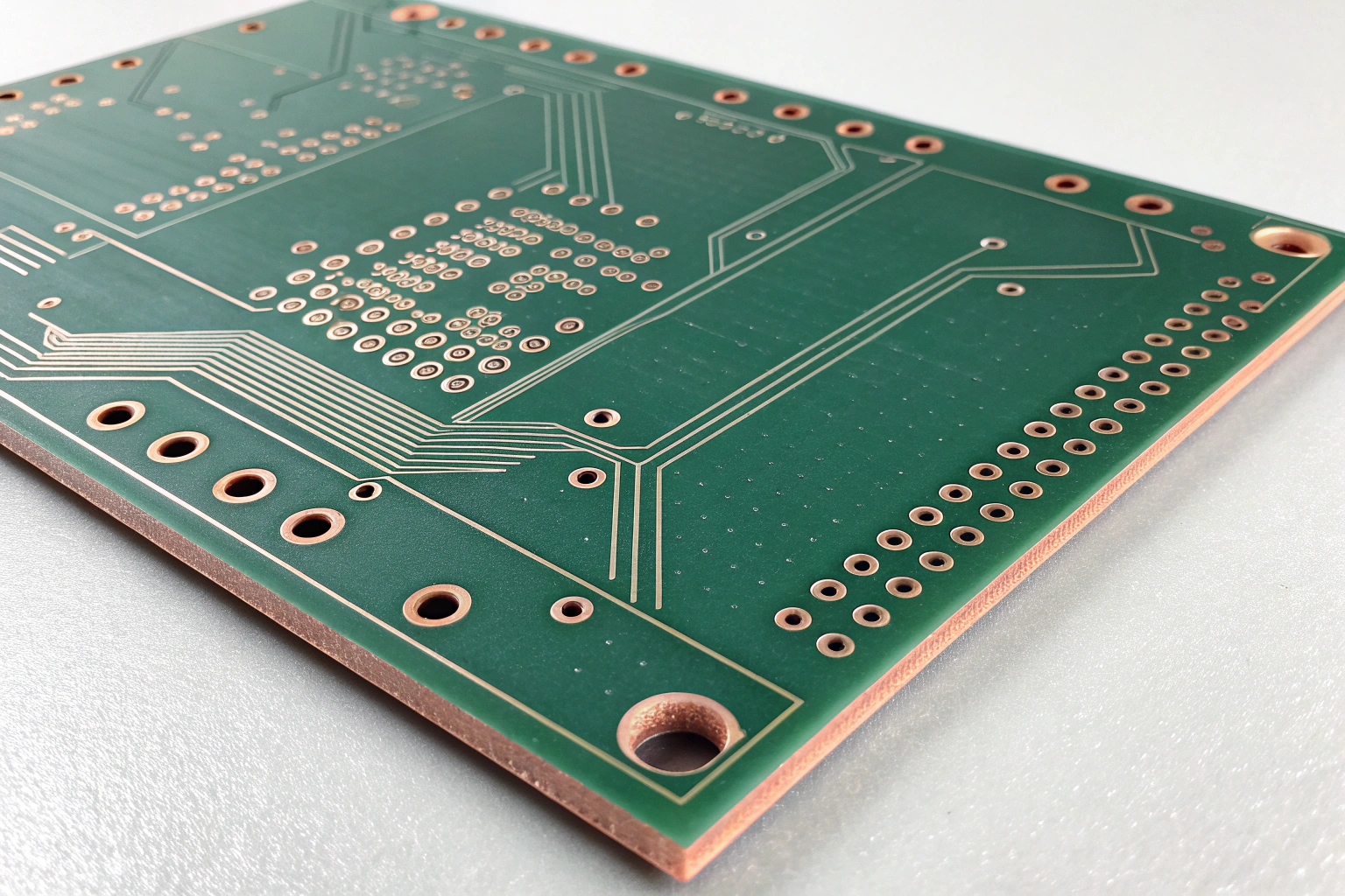
Balanced Layout and Professional Routing
Good boards look organized.
Order usually means good engineering.
High grade circuit boards show:
- Even trace widths and spacing
- Smooth, well-routed signal paths
- Proper separation of power, signal, and ground
- Logical component grouping
There is no random routing or unnecessary sharp angles. High-current paths are wider and reinforced. Sensitive signals are kept away from noise sources.
From a manufacturing perspective, balanced layouts heat evenly during soldering. This reduces solder defects and thermal stress.
Well-designed boards also survive rework and thermal cycling better, which is a key trait of high grade products.
Strong Mechanical Integrity and Flatness
Quality boards remain stable.
They do not bend or delaminate easily.
A high grade circuit board:
- Remains flat after soldering
- Shows no warping or twisting
- Has strong pad adhesion
- Shows no blistering or delamination
Connectors and heavy components are mechanically supported. Pads do not lift during rework. The board feels solid, not fragile.
This comes from:
- Proper laminate selection
- Correct Tg and material stack-up
- Controlled thermal profiles
- Gentle depaneling methods
Mechanical stability is essential for vibration resistance, connector reliability, and long service life.
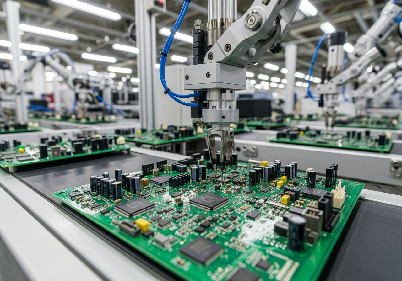
Evidence of Controlled Factory Manufacturing
High grade boards reflect system-level discipline.
Quality is built, not inspected in later.

A high grade circuit board shows signs of a controlled manufacturing environment:
- Consistent quality across samples
- No random variation between boards
- Clear inspection marks and traceability
- Stable results during testing
Behind this appearance is a factory workshop with:
- ESD-controlled production lines
- Calibrated SMT and testing equipment
- Defined process parameters
- Trained operators and engineers
Inspection systems such as SPI, AOI, X-ray, and functional testing support this consistency. Defects are prevented early, not corrected later.
High grade boards do not rely on rework to look good. They are right the first time.
Conclusion
A high grade circuit board looks clean, precise, flat, and consistent, with uniform solder joints, accurate component placement, controlled surface finish, and organized layout. These visual traits reflect deeper qualities: stable materials, disciplined manufacturing processes, and strong engineering control. In professional manufacturing, high grade PCBs are not defined by appearance alone, but by repeatability, reliability, and long-term performance. When a circuit board looks orderly and consistent across every detail, it usually means the factory behind it is equally disciplined. This is what separates truly high grade circuit boards from those that only look acceptable at first glance.
